Demystifying CXL Memory Interleaving and HDM Decoder Configuration
Memory interleaving is a technique that distributes memory addresses across multiple memory devices or channels. Instead of storing data sequentially in one device, the system alternates between devices at a fixed granularity. It could help improve bandwidth, reduce latency, and enhance scalability. In the context of Compute Express Link (CXL), memory interleaving is facilitated by the HDM (Host-Managed Device Memory) Decoder.
The CXL HDM decoder enables the routing of both CXL.mem and UIO transactions targeting HDM. HDM Decoders are responsible for translating incoming Host Physical Addresses (HPA) into corresponding Device Physical Addresses (DPA), allowing memory accesses to be correctly directed to the appropriate device.
HDM decoders are mandatory for:
- CXL logical devices
- CXL type3 devices that are not RCDs
- CXL upstream switch ports
- CXL host bridge registers in CHBCR
System software can configure HDM decoders to control how memory is interleaved across CXL.mem-capable devices, enabling flexible and efficient memory mapping.
If no HDM decoders are programmed, CXL devices will fall back to using the CXL DVSEC range registers, which should be configured with the appropriate DPA range to ensure proper memory access.
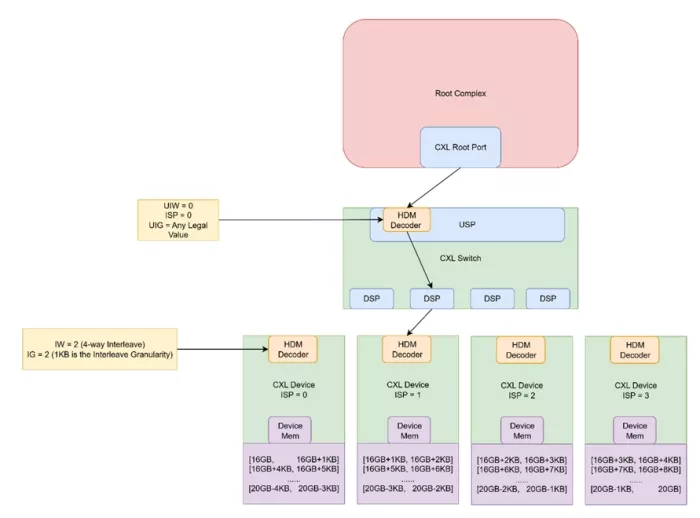
An Example of CXL Memory Interleaving and HDM Decoder
The following illustrates a simple memory fan-out topology with four memory devices behind a CXL switch. HDM decoder in each device, as well as the upstream switch port, is configured to decode the HPA range 16 GB to 20 GB, at 1-KB granularity. The leftmost device receives 1-KB ranges starting with HPAs 16 GB, 16 GB + 4 KB, 16 GB + 8 KB, …, 20 GB – 4 KB (every 4th Chunk). The root complex does not participate in the interleaving process.
Key Concepts Explanation
Interleave Way (IW): The number of memory units involved in a memory interleaving scheme. In CXL, an interleave set may contain either 1, 2, 3, 4, 6, 8, 12, or 16 CXL devices. 1-way interleave is equivalent to no interleaving.
Interleave Granularity (IG): Each device in an interleave set decodes a specific number of consecutive bytes, referred to as chunk, in HPA space. The size of the chunk is known as an interleave granularity. The starting address of each chunk is a multiple of IG.
Target: The HDM decoders in the CXL host bridge are responsible for looking up the incoming HPA in a CXL.mem transaction and forwarding the HPA to the appropriate root port target. The HDM decoders in the CXL upstream switch port are responsible for looking up the incoming HPA in a CXL.mem transaction and forwarding the HPA to the appropriate downstream switch port target.
Interleave Set Position (ISP): The position of this component in the interleave set formed when all HDM decode stages that are upstream of this port are considered. Expressed as a 0-based quantity.
The above parameters are configurable in CXL HDM decoder capability structure.
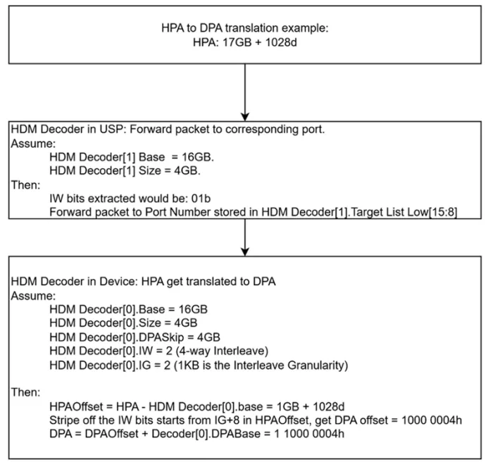
An Example of HPA to DPA Translation
Let’s use the above topology as an example and perform one HPA to DPA translation on one CXL.mem TL packet.
When a Host Physical Address (HPA) is deemed invalid—such as being outside the expected address range—the system may respond in one of several ways, depending on the capabilities of the device:
- MemData-NXM (Non-eXistent Memory) response
- Poisoned data response
- All 1s data response
Rules of Programming HDM Decoder
Some rules need to be followed when programming an HDM decoder. These rules help to ensure that HDM decoders being used will function properly.
- Decoder[m+1].Base ≥ (Decoder[m].Base+Decoder[m].Size). This ensures that the base of the decoder being committed is greater than or equal to the limit of the previous decoder. This check is not applicable when committing Decoder 0.
- Decoder[m+1].Base ≤ Decoder[m+1].Base+Decoder[m+1].Size (no wraparound)
- If Decoder[m+1].IW ≥ 8, Decoder[m+1].Size is a multiple of 3.
- Target Port Identifiers for Interleave Way=0 through 2**IW –1 must be distinct. This ensures no two interleave ways are pointing to the same target.
- Decoder[m].Committed=1. This ensures that the previous decoder is committed and has passed the above checks.
UIO Direct P2P to HDM
CXL.mem devices that can complete UIO requests targeting their HDM advertise the capability via the UIO-capable bit in the CXL HDM decoder capability register.
A UIO address is considered valid if at least one HDM decoder instance is capable of correctly processing the associated UIO transaction. This means the address must be a translated address, and the entire range of the UIO packet must fall within the bounds defined by the decoder and not crossing interleave boundary. A completer abort would be returned if there’s not a full match.
Further details on the matching rules and conditions can be found in section 9.16.1.1 and 9.16.1.2.
Simplifying HDM Decoder and Memory Interleaving with VIP
While HDM decoding and memory interleaving are central to unblocking the full potential of CXL, their inherent complexity can pose challenges for validation and integration. Our VIP (Verification IP) solution is designed to streamline this process, offering flexible configuration and a simplified reprogramming flow for HDM decoders.
Key Features of VIP
- Configuration validation
Automatically verifies that HDM decoder setup is correctly applied. - HPA-to-DPA translation trace
Provides a complete and transparent mapping from host physical address to device physical address. - Switch-aware HDM decoder support
Enables accurate modeling and testing of HDM decoders in switch-based topologies.
By leveraging these capabilities, customers can more effectively validate their designs, reduce debugging time, and ensure robust memory interleaving behavior across CXL.mem-capable devices.
More Information
- For more information about how Cadence PCIe/CXL Verification IP and TripleCheck enable users to confidently verify disruptive changes, see Simulation VIP for CXL, Simulation VIP for PCIe, and TripleCheck for PCIe and CXL
- For the press release on CXL3.0, please read Cadence's CXL 3.0 Verification IP Press Release
- For more information on CXL in general, please visit the CXL Consortium website
- If you have more feedback or need more information, reach out to us at talk_to_vip_expert@cadence.com"
Related Semiconductor IP
- CXL 4 Verification IP
- VIP for Compute Express Link (CXL)
- CXL 3.0 Controller
- CXL Controller IP
- CXL memory expansion
Related Blogs
- De-mystifying CXL: An overview
- Accessing Memory Mapped Registers in CXL 2.0 Devices
- PLDA and AnalogX Acquisitions Supercharge the Rambus CXL Memory Interconnect Initiative
- Accelerating the CXL Memory Interconnect Initiative
Latest Blogs
- Area, Pipelining, Integration: A Comparison of SHA-2 and SHA-3 for embedded Systems.
- Why Your Next Smartphone Needs Micro-Cooling
- Teaching AI Agents to Speak Hardware
- SOCAMM: Modernizing Data Center Memory with LPDDR6/5X
- Bridging the Gap: Why eFPGA Integration is a Managed Reality, Not a Schedule Risk