AI workloads demand smarter SoC interconnect design

Artificial intelligence (AI) is transforming the semiconductor industry from the inside out, redefining not only what chips can do but how they are created. This impacts designs from data centers to the edge, including endpoint devices such as autonomous driving, drones, gaming systems, robotics, and smart homes. As complexity pushes beyond the limits of conventional engineering, a new generation of automation is reshaping how systems come together.
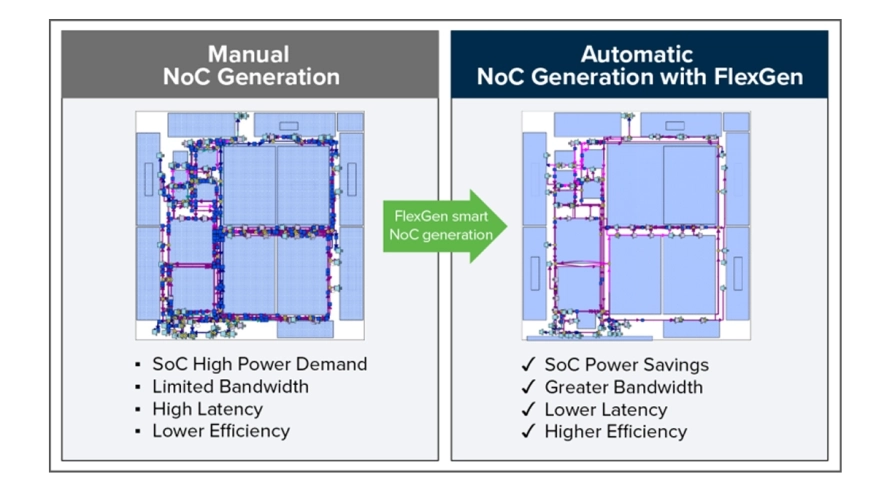 Instead of manually placing every switch, buffer, and timing pipeline stage, engineers can now use automation algorithms to generate optimal network-on-chip (NoC) configurations directly from their design specifications. The result is faster integration and shorter wirelengths, driving lower power consumption and latency, reduced congestion and area, and a more predictable outcome.
Below are the key takeaways of this article about AI workload demands in chip design:
- AI workloads have made existing SoC interconnect design impractical.
- Intelligent automation applies engineering heuristics to generate and optimize NoC architectures.
- Physically aware algorithms enhance timing closure, reduce power consumption, and shorten design cycles.
- Network topology automation is enabling a new class of AI system-on-chips (SoCs).
Machine learning guides smarter design decisions
As SoCs become central to AI systems, spanning high-performance computing (HPC) to low-power devices, the scale of on-chip communication now exceeds what traditional methods can manage effectively. Integrating thousands of interconnect paths has created data-movement demands that make automation essential.
Related Semiconductor IP
- Smart Network-on-Chip (NoC) IP
- FlexNoC 5 Interconnect IP
- FlexNoC Functional Safety (FuSa) Option helps meet up to ISO 26262 ASIL B and D requirements against random hardware faults.
- Network-on-Chip (NoC)
- NoC Verification IP
Related Blogs
- 2024 Set The Stage For NoC Interconnect Innovations In SoC Design
- Smarter SoC Design for Agile Teams and Tight Deadlines
- Introducing Open Access: SoC design for everyone
- Delivering a Secure, Cloud-Based SoC Design Environment for Aerospace Chip Designers
Latest Blogs
- A Bench-to-In-Field Telemetry Platform for Datacenter Power Management
- IDS-Verify™: From Specification to Sign-Off – Automated CSR, Hardware Software Interface and CPU-Peripheral Interface Verification
- RISC-V and GPU Synergy in Practice: A Path Towards High-Performance SoCs from SpacemiT K3
- EDA AI Agents: Intelligent Automation in Semiconductor & PCB Design
- Why Security Can't Exist Without Trust