LVDS IP
Welcome to the ultimate LVDS IP hub! Explore our vast directory of LVDS IP
All offers in
LVDS IP
Filter
Compare
232
LVDS IP
from
35
vendors
(1
-
10)
-
I/O Library with LVDS in SkyWater 90nm
- A SkyWater I/O Library combining standard GPIO, I2C-compatible ODIO, analog I/O, and integrated LVDS for robust mixed-signal and moderate-speed differ ential interfaces.
-
Automotive Grade PLLs, Oscillators, SerDes PMAs, LVDS/CML IP
- TSMC IP9000 Alliance member enabling automotive IP support in TSMC automotive processes
- Automotive Documentation including Safety Manual, FMEDA and DFMEA
- Design reliability report containing EM/IR and Aging analysis
-
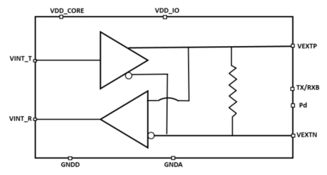
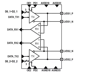
1 Gb/s LVDS Bidirectional IO on 12nm
- The ODT-LVDS-BID1G-12nm is a high-speed Bidirectional LVDS IO cell capable of operating up to 1 Gb/s.
- The ODT-LVDS-BID1G-12nm uses a high-speed signal path that can provide low jitter for input ranges of up to 1 Gb/s input.
- It also features small area and low power consumption.
- It includes the internal termination resistor and ESD protection diodes on the VEXTP and VEXTN pins.
-
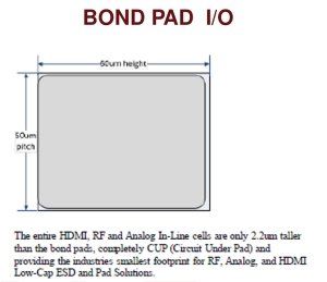
HDMI, LVDS, RF and Analog Pads in TSMC 45/40nm
- A 1.0V to 5V Analog I/O library that includes an HDMI, LVDS, and Analog/RF Low Capacitance pad set in TSMC 45/40nm HPM process.
- This library is collection of analog only IO and Power/Ground pads that include ESD. The target applications are high performance analog interfaces including HDMI, RF, LVDS, basic analog and other applications.
- The pads include a host of specialty features including fail safe, low capacitance, high ESD protection, and IEC robustness.
-
Library of LVDS IOs cells for TSMC 40LP
- TSMC 40 LP
- 2.5V/1.1V IO/Core transistors
- Fully compliant with TIA/EIA-644-A-2001

-
Library of LVDS IOs cells for TSMC 65LP
- TSMC 65 LP
- 2.5V/1.2V IO/Core transistors
- Fully compliant with TIA/EIA-644-A-2001
-
Rad-Hard GPIO, ODIO & LVDS in SkyWater 90nm
- This Library, developed on SkyWater 90nm CMOS, delivers a radiation-hardened suite of robust interfaces covering general-purpose, open-drain, and high-speed differential signaling needs.
- The GPIO provides reliable 3.3V digital I/O up to 150 MHz with JESD8C.01 compliance, built-in pull-ups/downs, and 2 kV HBM protection.
-
LVDS IO handling data rate up to 50Mbps with maximum loading 60pF
- KA16UGLVDS01ST001 is a LVDS IO handling data rate up to 50Mbps with a maximum loading of 60pF.
- The differential voltage swing can be programmable from 0.35V to 1V.
- The output enable control function can be activated to decide the IO as input/output function. This IP also includes the IO PAD.
-
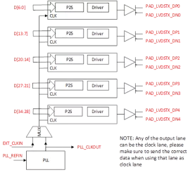
LVDS and OpenLDI PHY
- Silicon proven with maximum speed @1.5Gbps per lane
- Suitable for Automotive applications with ESD levels: HBM > 4KV and CDM > 750V
- LVDS TX PHY: 4-data lanes plus 1-clock lane with each lane can be individually turned off
- Supports long-distance transmission: Capable of maintaining signal integrity over longer cable length
-
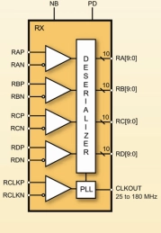
LVDS Deserializer IP
- The MXL-DS-LVDS is a high performance 4-channel LVDS Deserializer implemented using digital CMOS technology.
- Both the serial and parallel data are organized into four channels. The parallel data can be 7 or 10 bits wide per channel. The input clock is 25MHz to 165MHz. The De-serializer is highly integrated and requires no external components.