HDMI, LVDS, RF and Analog Pads in TSMC 45/40nm
A 1.0V to 5V Analog I/O library that includes an HDMI, LVDS, and Analog/RF Low Capacitance pad set in TSMC 45/40nm HPM process.
Overview
A 1.0V to 5V Analog I/O library that includes an HDMI, LVDS, and Analog/RF Low Capacitance pad set in TSMC 45/40nm HPM process.
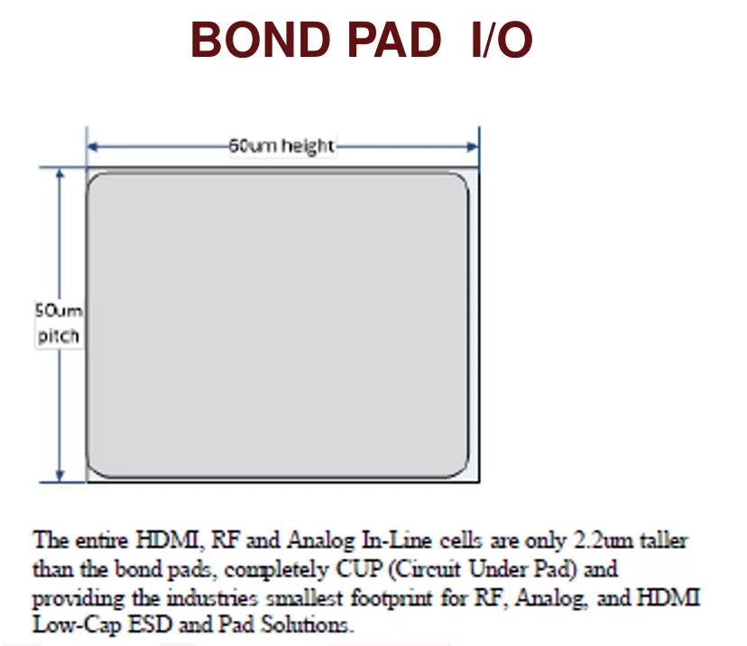
This library is collection of analog only IO and Power/Ground pads that include ESD. The target applications are high performance analog interfaces including HDMI, RF, LVDS, basic analog and other applications. The pads include a host of specialty features including fail safe, low capacitance, high ESD protection, and IEC robustness. The IOs are designed to trigger and protect interfaces during Electrical Overstress (EOS) events during normal operation. A key feature of the library is the extremely small footpr int of the inline IO set, only 2.2um bigger than the bond pad itself. Capacitance can range from <150fF to 250fF and is scalable based on the customers needs between ESD robustness and capacitive loading.
Key features
- In-line low-cap analog, 50um pitch x 60um height
- Dual-row, staggered pitch of 25um 150um height
- AVDD = 1.V to 3.3V nominal, 5V tolerant HDMI option
- Capacitance 150fF to 250fF including bond pads*
- HBM >4kV*, CDM >800V*, IEC >2kV option*
- EOS Protection
- Junction temperature range: -40C to 125C
- Can integrate with TSMC standard I/O
- HDMI and LVDS PAD Features
- Includes Power and Ground pads
- <250fF per I/O including bondpad
- 1.8V to 3.3V power supply (HDMI)
- 5V Tolerant (HDMI only)
- Fail-Safe I/O (HDMI only)
- Pad Macros provide ideal parasitic matching between differential signal pads
Block Diagram

What’s Included?
- Models and Support Files
- GDS Layouts
- LEF Abstracts
- CDL netlist for simulation and LVS
- Functional models in behavioral Verilog with timing arcs
- Front-end Devices
- 2.5V overdriven 3.3V thick-oxide NMOS and PMOS; No ESD implant layer or special masks required.
- Back-end: Metal 1 to Metal 8, AP bondpad layer for Wire-bond, using Circuit-Under-Pad construction.
Files
Note: some files may require an NDA depending on provider policy.
Silicon Options
| Foundry | Node | Process | Maturity |
|---|---|---|---|
| TSMC | 40nm | G | — |
Specifications
Identity
Provider

Learn more about Analog IP core
Analog Foundation Models
AnaFlow: Agentic LLM-based Workflow for Reasoning-Driven Explainable and Sample-Efficient Analog Circuit Sizing
Why Anti-tamper Sensors Matter: Agile Analog and Rambus Deliver Comprehensive Security Solution
Introducing agileSecure anti-tamper security portfolio
The Hidden Threat in Analog IC Migration: Why Electromigration rules can make or break your next tapeout
Frequently asked questions about Analog I/O Pad Library IP cores
What is HDMI, LVDS, RF and Analog Pads in TSMC 45/40nm?
HDMI, LVDS, RF and Analog Pads in TSMC 45/40nm is a Analog IP core from Certus Semiconductor listed on Semi IP Hub. It is listed with support for tsmc.
How should engineers evaluate this Analog?
Engineers should review the overview, key features, supported foundries and nodes, maturity, deliverables, and provider information before shortlisting this Analog IP.
Can this semiconductor IP be compared with similar products?
Yes. Buyers can compare this product with similar semiconductor IP cores or IP families based on category, provider, process options, and structured technical specifications.