Time-Domain Analog Design: Why and How
By Augustine Kuo, Seamless Microsystems
The widespread adoption of scaled CMOS process technologies has made battery-operated consumer devices more powerful, cheaper, and last longer. In the last two decades, CMOS technology scaling has resulted in orders of magnitude reduction in transistor sizes, from 90nm in 2004 to 7nm in 2019 and 3nm in 2024. However, as transistor dimensions reduce, in order to maintain the desirable transistor characteristics i.e. for the gate terminal to retain control over the transistor channel, the transistor gate oxide thickness also needs to be reduced. This in turn requires a steady reduction of the power supply for both core and I/O devices to guarantee reliability of the transistor gate oxide against breakdown.

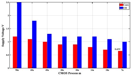
Fig. 1: Core and I/O supply voltage vs. CMOS scaling
In any CMOS process, there are two distinct types of transistors available: core and I/O. I/O transistors typically interface the IC with the outside world and have thicker gate oxide thickness and are longer. The core transistors implement the processing power. E.g. in a 28nm CMOS process, core transistors have a minimum 28nm gate length while I/O transistors have a minimum 130nm gate length. Fig. 1 shows the core and I/O power supply voltages as a function of the CMOS process node, with the supply voltage for core/IO devices shrinking from 1.2V/2.5V in 90nm to 0.65V/1V in 7nm, and is expected to shrink further with CMOS scaling to 5nm and 3nm.
Device and supply voltage scaling with technology greatly benefits digital circuits, where transistors are configured to operate as ON or OFF switches. As the transistors becomes smaller, they switch faster. Smaller transistors result in smaller device parasitic capacitances and die area, and smaller supply voltages result in a drastic decrease in switching power (proportional to square of supply voltage), and hence lower power consumption. Small die area and low power enables the use of cheaper chip packages, thus bringing the total cost down [1].

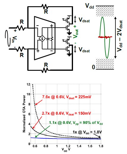
Fig. 2: (a) Typical 2-stage resistive feedback amplifier (b) Amplifier power vs. supply voltage
However, analog and mixed-signal (AMS) circuits face a number of challenges as a result of technology scaling. In AMS designs, transistors are required to operate in the transition region between fully ON and fully OFF (the linear region of operation). The shrinking power supply reduces the maximum available signal swing in AMS circuits, thus reducing the maximum achievable signal-to-noise ratio, a very important metric for high-performance AMS designs. Amplifiers with large gain configured in negative feedback are the basic building block of AMS designs. CMOS scaling reduces the transistor intrinsic gain, due to drain induced barrier lowering (DIBL). This in turn makes it very hard to achieve large gains with amplifiers designed in scaled CMOS technologies. The shrinking voltage supply also reduces the available device voltage headroom making it infeasible to achieve large gains by device stacking.
To illustrate the effect of supply scaling on the design of conventional analog circuits, Fig. 2(a) shows a typical 2-stage operational transconductance amplifier (OTA, commonly called an op-amp) configured as a resistive negative feedback amplifier. The amplifier consists of a 1st stage integrator followed by a class- A output stage. The maximum signal swing (single-ended peak-to-peak) Vout at the output of the amplifier is limited by the voltage headroom required by the output stage transistors which are typically biased in saturation. This maximum signal swing is limited to Vdd − 2Vdsat, with the transistor drain saturation voltage Vdsat typically 150mV or more. The voltage headroom required by the output stage severely limits the signal swing, which reduces from 1.5V at a supply of 1.8V in 0.35m CMOS process to just 0.3V at a supply of 0.6V in a 7nm CMOS process, a 5 times decrease in signal swing or a 13.5dB loss in maximum available signal power at 0.6V. The power consumed by the amplifier of Fig. 2(a), plotted in Fig. 2(b) as a function of the power supply, is the sum of the power consumed by the 1st stage integrator, which is noise-limited and dominates at low supply voltages (due to the limited signal swing) and the power consumed by the output stage, which is efficiency limited and dominates at high supply voltages. It can be seen the power consumed rises quadratically with reducing signal swing at lower supply voltages.
As a result of various challenges faced by AMS designs in scaled CMOS technologies, such designs are typically done in older CMOS technologies with higher supply voltages or using I/O devices with larger supply voltages, both significantly increasing the power consumption and cost. In System-on-Package (SOP) designs, it is sometimes impractical, from a cost point of view, to have analog and digital dies fabricated in different technology nodes. Since the digital portions overwhelm the analog portions in terms of area, the analog circuits must be designed in the same technology node as their digital counterparts. Thus, the design of AMS circuits in scaled technologies requires a number of innovative techniques to overcome scaling challenges. As shown in Fig. 2(b), if the amplifier is able to support a 90% supply signal swing at its output, then almost no extra power is required to achieve a particular SNR at low supply voltages. Seamless Microsystems’ Switched-Mode Signal Processing (SMSP) makes this possible. Vdd 0 Analog Signal Pulse-width encoded signal Switched-Mode Signal Processing t

Fig. 3: Switched-Mode Signal Processing output waveform
SMSP is a revolutionary paradigm for the design of high-performance analog circuits in scaled CMOS processes. Conventional AMS designs encode signal information in the voltage or current domains: a large signal is represented by a large voltage/current and a small signal is represented by a small voltage/current. SMSP encodes signal information in the time domain using pulse-widths, rather than currents or voltages, to leverage the faster switching speed of transistors. Switched-Mode Operational Amplifiers (SMOA) are multi-stage amplifiers implemented using SMSP.
Fig. 3 shows the sample output waveform of a 1-phase SMOA amplifying a sine-wave. The signal, a sine-wave in this case, is encoded in terms of pulse-widths, enabling high-resolution analog design by primarily using switches. Since SMOAs exploit the switching speed of transistors in scaled CMOS, the performance of SMOAs gets better with CMOS scaling, in direct contrast to conventional design techniques. Since SMOAs encode signal information in pulse widths at their output, the maximum signal swing of SMOAs is limited only by the minimum pulse width that the circuits can represent. The peak output swing of an SMOA can be easily shown to be Vdd *(1−2tminFSMOA), where tmin is the minimum pulse width that the SMOA can represent and FSMOA is the SMOA reference frequency. In 16nm CMOS, at a Vdd of 0.7V, with tmin of 50ps and FSMOA of 300MHz, the peak signal swing can be as high as 97% of Vdd, a 2.3× improvement in signal swing when compared to the classical OTA of Fig. 2 and Vdsat of 200mV.
SMOAs are analogous to class-D audio power amplifiers with high power-efficiency and high-resolution. But, unlike class-D audio amplifiers which are limited to bandwidths of <200KHz, SMOAs can process bandwidths in excess of 10GHz. Seamless Microsystems’ patented SMSP technology has been used to develop continuous-time filters [1] [2], and since the technology is a basic building block for all analog designs, it has also been applied to high speed receive paths for serial links (SERDES), Analog-to-Digital Converters (ADCs) and Power Amplifiers (PAs).

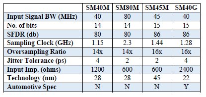
Table I: SMI’s 1st generation ADC portfolio
Table I shows SMI’s 1st generation portfolio of high-speed continuous-time delta-sigma ADCs built using SMSP. Continuous-time oversampled ADCs result in significant cost reduction, very relaxed anti-alias filters, being easier to drive and achieving large clock jitter tolerance. SMI’s use of SMSP technology results in ADCs requiring only a single core supply voltage, greatly simplifying system integration. SMI’s Si-proven SM40M [4] and SM80M ADCs achieve best-in-class performance and find use in wireless communications and medical imaging applications. SM45M was developed for use in a multi-channel ADC array for ultrasonic medical imaging.

Table II: SMI’s 2nd generation ADC portfolio
Table II shows SMI’s 2nd generation continuous-time delta-sigma ADCs, based on SMI’s revolutionary 2-step SMSP architecture. These ADCs have an order of magnitude wider bandwidth than SMI’s 1st generation ADCs and find applications in high-speed LiDAR sensors for autonomous driving and advanced driver assistance systems. Another example application of SMI’s 2nd generation ADCs are in wideband 5G wireless communications. For 5G, the number of base stations will increase and with the number of antennas also increasing for each base station, there will be over 128 channels per base station. If conventional ADCs are used for digitizing the data streams, they would consume an order of magnitude of power more than ones built with SMI’s technology.
To summarize, current analog design techniques are not well suited for the newest CMOS technologies. This has resulted in either a separation of analog and digital chips or using higher supplies for the analog portion in an integrated system-on-chip. In both cases, they would consume more power than an integrated solution that just used the core power supply. SMI’s patented technology allows analog designs to use the latest CMOS technologies in the lowest voltage supplies which results in smaller die areas and lower power. [1] J. Kuppambatti, "Design Techniques for Analog-to-Digital Converters in Scaled CMOS Technologies," 2014. [Online]. Available: https://academiccommons.columbia.edu/doi/10.7916/D8RV0KT8.
[2] J. Kuppambatti, B. Vigraham and P. Kinget, "A 0.6V 70MHz 4th-order continuous-time Butterworth filter with 55.8dB SNR, 60dB THD at +2.8dBm output signal power," in ISSCC, 2014.
[3] B. Vigraham, J. Kuppambatti and P. R. Kinget, "Switched-Mode Operational Amplifiers and Their Application to Continuous-Time Filters in Nanoscal CMOS," IEEE JSSC, 2014.
[4] Seamless Microsystems, "SM40M and SM80M datasheets: Available upon request from info@seamlessmicro.com," [Online].
Related Semiconductor IP
- DeWarp IP
- 6-bit, 12 GSPS Flash ADC - GlobalFoundries 22nm
- LunaNet AFS LDPC Encoder and Decoder IP Core
- ReRAM NVM in DB HiTek 130nm BCD
- UFS 5.0 Host Controller IP
Related Articles
- Agile Analog's Approach to Analog IP Design and Quality --- Why "Silicon Proven" is NOT What You Think
- How to Elevate RRAM and MRAM Design Experience to the Next Level
- Advanced Topics in FinFET Back-End Layout, Analog Techniques, and Design Tools
- Simplifying analog and mixed-signal design integration
Latest Articles
- Assertain: Automated Security Assertion Generation Using Large Language Models
- VolTune: A Fine-Grained Runtime Voltage Control Architecture for FPGA Systems
- A Lightweight High-Throughput Collective-Capable NoC for Large-Scale ML Accelerators
- Quantifying Uncertainty in FMEDA Safety Metrics: An Error Propagation Approach for Enhanced ASIC Verification
- SoK: From Silicon to Netlist and Beyond Two Decades of Hardware Reverse Engineering Research