Modular Design Of Level-2 Cache For Flexible IP Configuration
By Thang Tran, Synopsys Inc.
Abstract:
The microprocessor-memory gap has been growing for over 30 years, and in that time caches have been crucial components in digital system design. All high-performance microprocessors are designed with level 1 and level 2 caches, and multicore systems include many hierarchical levels of caches. The internet of things (IoT) along with the proliferation of portable devices are a major thrust for high-end embedded systems thus the need for higher performance processors and multicore; even little flash drives include multicore systems-on-chip (SoCs). As a result level 2 cache is becoming important in embedded designs. This paper presents an innovative level 2 cache design that meets the requirements of flexibility, configurability, low power, and small area for embedded systems.
I. INTRODUCTION
My first cache design was more than 30 years ago, it was the 2 KB Branch Target Cache (BTC). We jokingly called it “Bill-The-Cat.” Every transistor was designed by hand, including the SRAM cell, the sense-amp, the pre-charged logic, the row decoder, the input/output drivers, and the state machine. Fast forward to today’s technology where level 2 (L2) cache is no longer a custom design. A memory compiler is used to generate the exact required array size with a great deal of flexibility for tag, status, and data arrays configurations. The L2 cache is fairly complex to design for all possible configurations and features. To a great extent, the memory hierarchy is the driving force behind processor proliferation, which has evolved from desktop and laptop PCs to smartphones, tablets, and automobiles; and on the horizon, Internet of Things (IoT) and embedded vision applications. This shift requires extensible and configurable microprocessors with an optimal balance of performance, power, and area (PPA). The L2 cache must evolve to provide flexible configurability with the lowest possible PPA to be incorporated into the configurable microprocessors.
II. BACKGROUND
A. Microprocessor Evolution
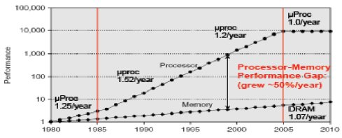
As soon as pipeline stages are added to a microprocessor design, the speed of the microprocessor improves at a much faster rate than the speed of the memory. As shown in Figure 1, processor speed was 200 times faster than the DRAM speed in the year 2000. Going to external memory takes hundreds of clock cycles, thus data fetch becomes critical for the microprocessor performance. The data dependency penalty is an obstacle to be solved by the microprocessor designers. The cache becomes an important feature for the microprocessor. The BTC is used to fetch the first two instructions internally, allowing the subsequent instructions to be fetched from the external memory. The cache memory evolves to multiple levels and the cache hierarchy is the most effective way to reduce the data fetch time. Current microprocessors for PCs, laptops, smart phones, and tablets have built-in cache hierarchy. The PCs and laptops are often advertised with the L2 cache size. Fig. 1. Microprocessor-Memory Performance Gap [1]

Fig. 1. Microprocessor-Memory Performance Gap [1]
B. L2 Cache Requirements
The first generation of microprocessors was driven by the high performance required by the PC and laptop market. Once the PC and laptop market became saturated, the requirements of the next generation of microprocessors was driven by mobile devices like smartphones and tablets, which require low-power microprocessors to enable longer battery life. Almost everyone has a cell phone worldwide and many have two, making the number of cell phones in use today more than the total population of the world [2]. The maturity of the tablet and smartphone market is evidenced by Apple announcing a drop in sales for the first time in 15 years. There is no obvious single next big application. The market is diverse with a wide range of applications with different requirements. The IoT, connected automobiles, wearables, medical devices, gaming, virtual devices, smart cities, building and factories are all driving a new and diverse set of processor requirements. The ability to configure and extend a processor to meet the requirements of the application is a promising new technology model for processors. It provides high degrees of flexibility, giving SoC developers the ability to include their own proprietary custom instructions. The SoC design can also reach the optimal tradeoffs in performance, power and area by customizing the processor IP to the application requirements. Also, the customization of processor technology provides the ability to meet evolving standards. With the wide variety of applications and requirements today, from consumer to automotive, there are just too many different types of applications to standardize on a single fixed processor IP.
Following the same trend, L2 cache must provide the flexibility in configuration for the SoC design. The configurations include cache size, the number of way-associative, the number of banks, the number of input ports with individual read/write configuration, flexible memory latency, power-down options, error correcting code (ECC) and parity, and cache partitioning. In order to adapt to all the requirements for L2 cache design, a new design methodology is necessary. The modular design method for L2 cache will be discussed in detail in subsequent sections. Cache coherency is another full topic by itself and will not be discussed in this paper. Throughout this paper, “configure” refers to the build-time configuration of the RTL for the L2 cache and “program” refers to the run-time options.
III. MODULAR DESIGN
The L2 cache design must provide the flexibility to be used in many different embedded systems and applications. Like microprocessor design, L2 cache has a pipeline, as shown in Figure 2. The requests traverse through the pipeline of the tag array and the data array to read and write data. The traditional design interlocks the requests through all the pipeline stages. The design becomes complex when considering the cache miss, the cache replacement, the data eviction, the prefetching of data and all the possible conflicts between them. The traditional design lacks the flexibility required for all the possible configurations needed for an embedded system.

Fig. 2. Typical 10-Stage Pipeline of the Level 2 Cache
A. Modular Design Concept
The modular design concept is breaking the L2 cache into independent units. The fixed pipelining concept is no longer important. Each unit processes its own function without interference from other units. The features of modular design are:
- The standard valid-and-accept request protocol is used for sending requests from one unit to another unit:
- A valid request must be accepted by the next unit, otherwise, the request is replayed
- Each modular unit consists of a queue and an execution block
- The unit can accept multiple requests into the queue
- A request enters the queue and sends to the execution block in order
- The execution block can have a variable cycle latency. A count-down counter decrements the cycle latency to zero before allowing the next request to enter the execution block
- The “issue and replay” protocol is used
- The concept is fire and forget. When the request is ready, it will be sent to the execution block. If there is an issue with execution, then the request will be replayed from the queue in order
- No stall and no interlock
- Each request has a tag ID to be tracked throughout the L2 cache
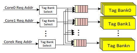
The tag bank unit in Figure 3 is an example of modular units. The tag bank is the execution block. The queue received requests from multiple cores and sends one request at a time to the tag bank. The tag bank can take 1 or more clock cycles to access data. The latency counter is used to allow the next request to access the tag bank. Each tag bank is an independent modular unit and each tag bank unit executes the requests from its own queue.

Fig. 3. Tag Bank Units
Modular design has the following advantages, which will be discussed in further detail in later sections.:
- The pipeline is not important. Each modular unit has its own configurable or programmable latency
- The modular unit can accept many different sources of requests by the same protocol. For example, the cache maintenance, the cache replacement, the cache eviction requests do not interrupt the 10 pipeline stages to access the tag array
- The modular unit uses the “issue and replay” protocol to avoid blocking other high priority requests, thus avoiding dead-lock in the design. For example, the cache maintenance, the cache replacement, the cache eviction requests can access the tag array at any time without interfering with normal requests
- The modular unit can be independently synthesized for timing, making performance more predictable
- The modular unit can be independently verified at the unit-level, reducing verification complexity
B. L2 Cache Modular Units
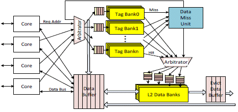
The overall view of the L2 cache is shown in Figure 4. The L2 cache is broken down into many modular units. Each data bank, each tag bank, and each input channel are individual modular units. Each modular unit independently executes the request and sends to the next modular unit.

Fig. 4. L2 Cache Block Diagram
The central unit of the L2 cache is the data buffer where the tag ID is assigned to individual request. As a new request is received, an entry in the data buffer, which will be used throughout the L2 cache, is assigned to the request. The data buffer consists of:
- A free-list indicates the available entries in data buffer. The free-list entry is assigned to the new request and the finished entry is reclaimed into the free-list
- Each data buffer entry is a cache line. The cache line represents the data input or output to the data banks of the L2 cache array. In addition to data, each entry has the request address and control information. The cache line size is convenient and without conflict for reading/writing data directly to the data banks from the input channel or the fetched data from the external memory. The data buffer is similar to the re-order buffer (ROB) of the superscalar and out-of-order microprocessor where each entry in the ROB is assigned to an instruction.
Other L2 cache modular units are:
- The read/write input-channel units, one modular unit per input channel. The requests enter a queue and execute in-order. The execution of the input request is reading and writing of the data buffer:
- Each request is assigned an entry in the data buffer. The read unit monitors the first packet of data in the entry, as the data is valid, it sends data back to the core and moves to the next packet of data.
- The write unit reads data from the input channel and writes to the assigned entry in the data buffer and sets the appropriate valid bit. The data bank unit is responsible to fetch the valid data and write to the data bank.
- The tag bank unit, one modular unit per tag bank. Each tag bank unit consists of a queue and a tag array. The tag bank unit is selected based on the bits of the address. Per valid request from the input channel, the request address is decoded and routed to the specific tag bank queue. The data buffer ID is also attached to the request to the tag bank queue. The queue executes the requests in-order. The tag array is accessed and checked for hit and miss determination as execution block. The tag hit forwards request to the appropriate data bank. The tag miss forwards the request to the data miss queue.
- The data bank unit, one modular unit per data bank. Each data bank unit consists of a queue and a data bank array. The data bank unit is selected based on the bits of the address. If the request is hit in the tag array, then it sends the request to the appropriate data bank queue based on the request address. The queue executes the requests in-order. For read request, it reads data from the data bank and writes to the data buffer entry using the data buffer ID. For write request, it reads valid data from the data buffer and writes to the data banks.
- The status bank unit, one modular unit per status bank. Each status bank unit consists of a queue and a status array. The requests from the tag bank unit enter the status bank queue and access the status array in order. The status consists of modify bits, lock bits, and pseudo-least-recently-used (PLRU) bits. The modify bits are set upon write requests from the core, the lock bits are set from the core command, and the PLRU bits are set on every read or write request.
- The data miss queue unit is a modular unit that receives tag miss requests from the tag bank units into a queue. The queue executes the miss requests in order. It sends speculative request to fetch the cache line from the external memory. The miss request will also access the status bank for replacement information. If eviction is needed, then the request is sent to the tag bank unit for eviction. The miss and eviction requests bypass the tag and status bank queues to access the tag and status arrays directly.
- The fetched data from the external memory for the miss request is sent directly to the Data Buffer. The process of writing the fetched data to the data banks is similar to the write request from the input channel, when the data is valid, it is written to the data banks.
- The eviction buffer unit is a modular unit that receives the evicted data from the data bank unit. The eviction unit executes the evicted data in order. When data is valid, then the write request is sent to the external memory.
IV. ADVANTAGES OF MODULAR DESIGN FOR L2 CACHE
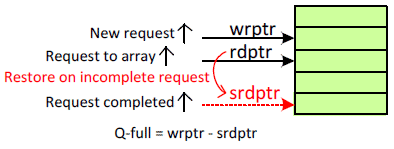
The modular design makes extensive use of the queue. The same queue structure is used in all units and is shown in Figure 5. The queue is a better alternative than the shift registers in terms of power. The data is written once to an entry instead of write and read to shift to the next entry. The data is retained until the execution is completed. The request can be replayed by moving the read pointer to the saved pointer.

Fig. 5. Queue Structure and Operation
A. Parallel Processing for Higher Performance
There are several advantages for the tag bank units in Figure 3:
- If the requests are to different tag bank units, then they can be executed in parallel, thus providing higher performance. Accordingly, the requests in the data bank units executes independently, allowing them to be executed out of order. Similarly, each channel unit is independent, allowing the valid data for each channel to return to the core out-of-order
- If the requests are to the same tag bank, then they can be accepted into the tag bank queue and delay the execution until the next cycle. The bottleneck is removed from the input channel, allowing the next request to be accepted and possibly sent to another tag bank queue
The modular design is similar to the reservation stations and functional units of the microprocessor. The requests are allowed to execute in parallel and out of order in different functional units.
B. Flexibility of Execution Latency
Synopsys’ DesignWare® ARC® HS cores are high-performance cores with L2 cache support. The L2 cache is designed to match the clock frequency of the ARC HS cores for easy interfacing and highest possible performance but the SRAM arrays can take multiple cycles to access data. The L2 cache can be configured with wide range of cache sizes from 128 KB to 8 MB. The access latencies are different for 128 KB and 8 MB caches. With modular design, the access latency is implemented with a simple counter. As the request is sent from the queue to the tag or data bank, the latency counter will count down to zero before allowing the next request to be accepted. This process is independent from all other units in the L2 cache. This simple mechanism of the latency counter allows further flexibility:
- High-density SRAM for low power/area has different a access time than high-speed SRAM for performance
- Different latency counter value can be used for different L2 cache sizes from 128 KB to 8 MB
- Additional cycle for ECC implementation, error correction is done by simply stalling the counter for one more clock cycle
- Adding an extra cycle latency for routing delay to individual data bank unit, timing path due to routing delay is fixed by simply adding an extra clock cycle to the execution latency. The data banks can have custom access latencies.
- Adding extra cycle latency for sharing the SRAM arrays with other memory controller units
The modular design is very flexible in memory access latency and timing. For example, the input-channel read unit does not care about where or when the data is received. As long as the data in the Data Buffer is valid, then the input-channel read unit sends the data back to the input channel. The valid data can be from data banks in 2-5 clock cycles or from the external memory in 100 clock cycles. The data banks can take additional clock cycles for ECC correction which is unknown to the input-channel read unit.
Basically, the modular design allows the memory access latency to be programmed or configured based on the requirements of the IP embedded design or application. In a way, this is similar to different execution times for the simple ALU and the complex ALU.
C. Hierarchical Architectural Clock Gating
The modular units are independently clock gated. For example, if there is no tag miss and no eviction, then the Data Miss Unit and Eviction Buffer Unit are clock-gated off to save power. The tag, data, and status arrays are organized with independent banks. The clocks for the banks are active only if there is a valid request for the bank. If a tag bank has no request, then it is clock-gated off to save power.
When there is no request from the cores, then the L2 cache is totally clock-gated off, except for the core interface buffer which remains on to receive requests from the cores. The clocks of the L2 cache units are sequentially enabled as needed to service the request.
D. Flexibility of Configuration
Each modular unit is independent. The queue of the modular unit can receive the input from one source or multiple sources, making configuration much simpler. Of course, there is a limitation to the number of configurations due to timing constraints. The particular configurations of this L2 cache are:
- The number of input channels is configured to 16 to allow flexibility in number of cores for multicore design.
- The tag and data banks are configured to allow concurrent accesses from the number of requests from the cores. The bank conflicts can be reduced to allow higher performance. The limit number of banks is 16 for tag banks and 32 for data banks.
- The L2 cache size is configured from 128 KB to 8 MB, in reality, the upper limit depends on what is verified. The execution latency increases to accommodate the required tag/data bank sizes.
- This cache design can be used as back-side L2 cache, L2 cache, or L3 cache. The L2 cache can select small memory size configurations while the L3 cache can select much larger sizes.
E. Hierarchical Synthesis and Unit-Level Verification
Additional benefits from the modular units are hierarchical synthesis and unit-level verification:
- In a normal design cycle, the verification time is often three times the design time. Each modular design unit can be independently verified at the unit level. It is much simpler and faster to hit all corner cases and possible configurations. The verification time is drastically reduced with unit level verification.
- An additional restriction for the modular unit is the input and output signals of the unit. If the input and output signals must be from the flops and/or to the flops, then the timing of the input and output signals are deterministic. Each modular unit is synthesized and floorplanned with certainty to meet the required clock frequency.
SUMMARY
The presented L2 cache has many considerations for low-power design and great flexibility for the embedded memory system. Yet because of the modular design, the L2 cache design was completed in a relatively short time with minimal resources. This L2 cache can be configured and programmed in many types of multicore systems and SoCs. While the small L2 cache of 128 KB can be used as back-side L2 cache for a single core, with the large configurable size of 8 MB and large number of input ports, it can also be used as the L3 cache in multi-cluster system. In the current diverse markets from IoT to automotive to high-end application, an extensible and configurable microprocessor is needed to achieve optimal PPA. The flexible L2 cache is an integral part of the next generation of microprocessors [3].
Many basic concepts of the modular design in the L2 cache are applicable to other design. The future designs of complex superscalar microprocessor and multithread processing units takes advantage of the modular design to improve on all design parameters of performance, clock frequency, area, power, time-to-market, scalability, and configurability.
REFERENCES
[1] Inouye, J., et. al., “Overcoming the Memory Wall,” Oregon State University, 2012.
[2] https://en.wikipedia.org/wiki/List_of_countries_by_number_of_mobile_phones_in_use
[3] Casey, F. and Tran, T., “Configurable Microprocessor for Life Essential Devices,” IP-SoC 2016
[4] “DesignWare ARCv2 ISA, Programmer’s Reference Manual for ARCv2 Processors.” ARC Synopsys, August 2016.
[5] “DesignWare ARC HS Series Databook,” ARC Synopsys, August 2016.
Related Semiconductor IP
- ReRAM NVM in DB HiTek 130nm BCD
- UFS 5.0 Host Controller IP
- PDM Receiver/PDM-to-PCM Converter
- Voltage and Temperature Sensor with integrated ADC - GlobalFoundries® 22FDX®
- 8MHz / 40MHz Pierce Oscillator - X-FAB XT018-0.18µm
Related Articles
- The role of cache in AI processor design
- The Growing Imperative Of Hardware Security Assurance In IP And SoC Design
- Open-Source Design of Heterogeneous SoCs for AI Acceleration: the PULP Platform Experience
- Assessing Design Space for the Device-Circuit Codesign of Nonvolatile Memory-Based Compute-in-Memory Accelerators
Latest Articles
- An FPGA-Based SoC Architecture with a RISC-V Controller for Energy-Efficient Temporal-Coding Spiking Neural Networks
- Enabling RISC-V Vector Code Generation in MLIR through Custom xDSL Lowerings
- A Scalable Open-Source QEC System with Sub-Microsecond Decoding-Feedback Latency
- SNAP-V: A RISC-V SoC with Configurable Neuromorphic Acceleration for Small-Scale Spiking Neural Networks
- An FPGA Implementation of Displacement Vector Search for Intra Pattern Copy in JPEG XS