I-fuse: Most Reliable and Fully Testable OTP
By Shine Chung, Chairman of Attopsemi™ Technology
Abstract:
OTP stands for “One-Time Programmable”, a device that can only be programmed once to store data permanently but ideally read infinite times. Traditionally, testability has been an issue for OTP. Every OTP bit should be programmed to ensure programmability. However, if only a single bit is programmed, the OTP block can no longer be used.
Patented by Attopsemi™, I-fuse™ is a revolutionary non-breaking fuse technology that can be reliably programmed by heat assisted electromigration below a break point. Any cell can be tested as programmable if the initial fuse resistance is low enough (e.g. <400 ohms) to generate enough heat for programming. The program voltage range can be tested and calibrated in a way that program yield can be predicted accurately. In I-fuse™ design, a pseudo-programmed state can be created by applying a low voltage programming during read, called Concurrent Low-Voltage Write Read (CLVWR). By combining the normal read and pseudo-programmed read, complex SRAM-like test patterns can be generated to fully test a complete I-fuse™ OTP macro with 100% fault coverage.
Introduction to OTP
OTP is used in many applications, for example, to customize a chip after fabrication, to store chip ID, firmware, security key, or configuration data, work around defect/contamination, trim device variations, or enable/disable certain functions. OTP is one of the four foundational IPs, along with I/O library, standard cell library, and SRAM compiler, that every customer needs to tapeout their chips to foundries for fabrication.
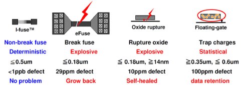
The conventional OTP programming concepts are based on storing or breaking something to create “permanent” programmed states. These mechanisms all have varying levels of deficiencies. Storing charges in a floating gate requires the gate oxide to be not too thick for charge injection and not too thin to retain charges. Rupturing gate oxide requires high voltage that may attract charges to trap in the gate oxide and can appear to breakdown, called soft breakdown. These charges can return to their original state after burn-in and the ruptured oxide can appear to be self-healed. Breaking an electrical fuse is equivalent to an explosion. During the programming, debris can be created and micro-bridged again becoming shorts. These types of OTP have severe reliability issues that need to implement redundancy, Error Correction Code (ECC), or twin cells.

Figure 1 : Summary of different OTP technologies
I-fuse™ is a revolutionary fuse-based OTP technology that limits program voltage to below breaking voltage so that only heat-assisted electro-migration takes place for programming. The reliability defect rate has been proven to be less than 1ppb without any type of redundancies. Different OTP technologies are summarized in Fig. 1.
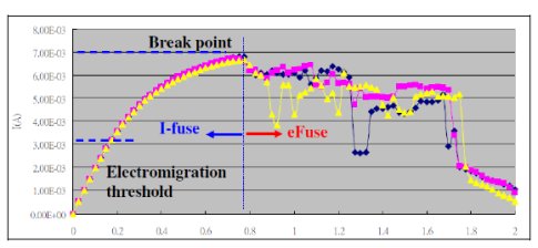
The comparison between conventional eFuse and I-fuse™ can be further explained. Fig. 2 depicts a typical current-voltage (I-V) curve for programming a fuse. When the applied voltage is higher, the current increases accordingly up to a certain point, called the break point. After this point, the current drops even if the voltage increases slightly. This will not take place unless the fuse breaks. There is a belief that a broken fuse can retain its program state forever. But actually the three fuses’ I-V curves shown in Fig. 2 behave differently beyond the break point. The programming is chaotic to the extent that the post-program fuse resistance can range from a few kilo-ohms to 1giga-ohm. On the other hand, if a fuse is programmed above an electro-migration threshold but below the break point, its behavior can be well predicted. The programming becomes orderly so that the post-program fuse resistance shows a nearly Gaussian distribution.

Figure 2: I-fuse™ versus eFuse in I-V curves of programming fuses.
ZERO defects
Instead of using testers for programming, it is becoming increasingly frequent and more important to program an OTP in the field, called field programming. In this case, any OTP programming failure or yield loss can be costly. There is a 10x rule as shown in Fig. 3. If a defect cannot be identified in wafer sort but goes to packaged chip, the cost may increase from $0.1 to $1. If a defect cannot be identified in the chip but makes its way to modules, the cost may go to $10. If a defect cannot be identified in the module but goes to printed circuit board, the cost may go to $100. Ultimately, if a defect is identified in the system, the cost may skyrocket to $1,000. That’s why there are increasing demands for “ZERO defects.” The true meaning of ZERO defects is to make sure no defects occur after shipping.

Figure 3: 10X cost to identify a defect in different product stages
Testability of OTP
Testability is vital for OTP to achieve ZERO defects. Before programming any OTP bits, the OTP readouts are all in a virgin state. Without programming any OTP bits, it would be difficult to ensure all bits can be programmable in field. But if only a single OTP bit is programmed, the OTP macro can no longer be used. This is the dilemma for OTP programming that Attopsemi™ has been able to solve.
There are 3 questions to be answered for OTP:
- How can you make sure the OTP shipped can be fully programmable?
- How can you make sure the OTP programming yield is nearly 100%?
- Can you test every functional block of OTP to make sure each block can perform as expected?
The answers of the above three questions are tied to the unique I-fuse™ programming mechanism. Unlike explosive programming behaviors in electrical fuse or anti-fuse, I-fuse™ programming is based on heat-assisted electro-migration below an explosive (break) point. If the initial I-fuse™ resistance can be tested to be low enough to generate sufficient heat, the I-fuse™ can surely be programmable in field. Therefore, a typical destructive programming test can be replaced by a non-destructive resistance screening. Any I-fuse™ with initial fuse resistance lower than 400 ohm, for example, can be guaranteed programmable. This is unique to I-fuse™. Conventional eFuse cannot guarantee programmability even if the initial fuse resistance is low enough due to chaotic and unpredictable program behavior.
Other OTP technologies, such as floating gate, electrical fuse, or anti-fuse have yield loss when programmed in field. Typically 1-2% of yield loss is not unusual because the programming mechanisms are based on applying high voltage or high current to break or to trap something in brutal forces. However, I-fuse™ programming has a well-defined program window of above electromigration threshold and below explosive (break) point. If any I-fuse™ is programmed within this program window, the programming behavior can be characterized, and the yield can be accurately predicted.
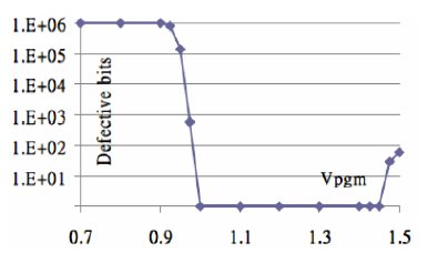
The program window can be characterized in a straightforward way. The minimum program voltage is determined by starting with a low programming voltage and incrementing until all bits can be successfully programmed. Incrementing the program voltage until at least one unprogrammed bit becomes programmed or one programmed bit becomes unprogrammed, the immediate previous program voltage is the maximum program voltage. As long as the maximum and minimum program voltages are wide apart and within the controlled margins, the program yield can be guaranteed to be 100%. A typical program defect versus program voltage in GlobalFoundries’ 22FDX® is shown in Fig. 4. Based on the test data, the program defect rate (called Bit Error Rate, BER) can be characterized very well.

Fig. 4 I-fuse™ program window characterization in GlobalFoundries’ 22FDX®
Concurrent Low Voltage Write Read
The last question above is about how to make sure every functional block of an OTP can perform as expected. Other than whether an OTP cell can be programmed or not, how to make sure sense amplifiers actually detect a programmed state? How to test if there are any Wordlines (WL) or Bitlines (BL) opens or shorts? How to test if all X- and Y- decoders identify unique addresses correctly? How to test if control logic functions properly? And the most important question: how to make sure program circuits do not accidentally program any bits during tests?
The above questions are simple to address for memories (such as SRAM or DRAM, for example) that can be read and written multiple times repetitively by using complex test patterns, such as March patterns, by reading and writing opposite data alternately. Any stuck-at faults or coupling faults can be detected easily. However, OTP can only be written once. Even if some spare bits in OTP macros can be tested during programming, there is still no guarantee the OTP bits in the main array will function as expected.
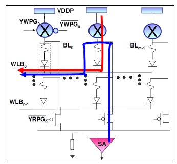
A non-destructive program state can be created in I-fuse™ so that the conventional memory test schemes can be applicable to exercise full fault coverage by generating SRAM-like test patterns. Clarification about the I-fuse™ OTP array structure in Fig. 5 can help to further explain this.

Figure 5: I-fuse™ array structure
Like other memory structures, an OTP has n-row and m-column of OTP cells arranged in a two-dimensional array. If a 1R1D (one resistor, one diode) cell is used as an example, all the cathodes of the diodes are connected together as Wordline Bar (WLB). And all the free ends of the I-fuse™ are connected together as Bitline (BL). Accessing any OTP cell for program or read can be through enabling the WLBs and BLs, which act as X and Y selects, respectively. For example, if a WLB and an YWPG (Y-Write-Pass Gate) are both selected, the corresponding cell can be programmable if a high voltage is applied to VDDP. Similarly if a WLB and an YRPG (Y-Read-Pass Gate) are both selected, the corresponding cell resistance can be read if a sense amplifier is turned on. If an I-fuse™ resistance is low before programming, the bitline voltage will be low so that the read data would be 0. However, if an I-fuse™ resistance is high after programming, the bitline voltage will be high so that the read data would be 1. Normally, programming and reading an OTP is mutually exclusive: when an OTP cell is being programming, there is no need to read. Conversely, when an OTP cell is being read, there is no need to program. What happens when both program and read are applied to the same cell, while the “program” voltage is low enough?
In this case, the bitline voltage will be pulled higher so as to read as data 1, the program state, even for a virgin fuse. Since the “program” voltage applied is very low, no actual programming can happen. Thus, a pseudo-programmed state is created but the cell is not actually programmed. This novel test scheme developed by Attopsemi™ is called Concurrent Low-Voltage Write Read (CLVWR). With this innovative scheme, any OTP cell, cell array, WLB/BL open/short, X-/Y-decoders, control logic, or even program circuits can be tested thoroughly.
In addition to full testability which is now required by many applications such as automotive, I-fuse™ also offer other multiple benefits such as smaller silicon area without charge pumps, programmable at core or I/O voltage, ultra-low energy readable with 0.4V/1uW for RFID or energy harvest, 250oC and even 300oC qualified without any kinds of redundancies, higher temperature, faster programming and reading speeds and lower current consumption.
Conclusion
One-Time Programmable (OTP) memories are commonly believed to be non-volatile memory requiring explosion or brute force in order to be permanently programmed. However, Attopsemi™’s I-fuse™ OTP is proven under a non-breaking program mechanism to have better results: small macros without charge pumps, low program voltage/current and low read voltage/current, high reliability, and wide temperature applications. Furthermore, I-fuse™ is also proven to be fully testable just like other logic circuits. Programmability of an I-fuse™ can be tested on initial I-fuse™ resistance. Program yield can be predicted very accurately by calibrating the program window. Finally, every functional block can be fully tested by employing Concurrent Low Voltage Write Read (CLVWR) to read and write unprogrammed and pseudo-programmed states alternately. From every aspect, I-fuse™ is a true logic device, instead of a nonvolatile memory, so I-fuse™ doesn’t need to be qualified as such. When a logic process is qualified, I-fuse™ is qualified.
I-fuse™ has been qualified and is now in volume production with multiple foundries and technologies ranging from 0.5μm to below 10nm, including BCD and SOI.
I-fuse™ is therefore the ultimate OTP.
References
[1] Shine Chung, et al, “Ultra-small and Ultra-reliable Innovative Fuse Scalable from 0.35um to 28nm”, IEEE ICMTS Feb., 2016.
[2] Shine Chung, “4K8 Innovative Fuse on 22nm FD-SOI”, IEEE J. Elec. Dev. Soc (open access)
Related Semiconductor IP
- NPU IP Core for Mobile
- MSP7-32 MACsec IP core for FPGA or ASIC
- UHF RFID tag IP with 3.6kBit EEPROM and -18dBm sensitivity
- NPU IP Core for Edge
- Specialized Video Processing NPU IP
Related White Papers
- I-fuse OTP - The OTP of Choice
- SRAM PUF: A Closer Look at the Most Reliable and Most Secure PUF
- Optimal OTP for Advanced Node and Emerging Applications
- Interstellar: Fully Partitioned and Efficient Security Monitoring Hardware Near a Processor Core for Protecting Systems against Attacks on Privileged Software
Latest White Papers
- Ramping Up Open-Source RISC-V Cores: Assessing the Energy Efficiency of Superscalar, Out-of-Order Execution
- Transition Fixes in 3nm Multi-Voltage SoC Design
- CXL Topology-Aware and Expander-Driven Prefetching: Unlocking SSD Performance
- Breaking the Memory Bandwidth Boundary. GDDR7 IP Design Challenges & Solutions
- Automating NoC Design to Tackle Rising SoC Complexity