I-fuse OTP - The OTP of Choice
By Shine Chung, Attopsemi Technology
Hsinchu, Taiwan, R.O.C.
Abstract :
OTP stands for “One-Time Programmable”, a device that can only be programmed once to permanently store any kind of information (data for chip IDs, security keys, product feature selection, memory redundancy, device trimming, or MCU code memory). Every chip needs OTPs, as long as they are reliable, available, and affordable.
I-fuse™ technologies achieve 100x reliability, 1/100 cell size, and 1/10 program current of the ubiquitous e-fuse, by (a) using junction diode, instead of MOS as a program selector in an OTP cell, (b) setting program current below a catastrophic breaking point, and (c) using small cell to increase program efficiency to reduce program current. As a result, our I-fuse™ can guarantee 0% program defect and can have less than 0.01ppm pre-program defect. Our I-fuse™ also passed data retention at 300oC for 1,000 hours. Our OTP can be programmed in low and standard voltages and can be available and scalable from 0.5µm to 28/20/16nm CMOS.

Fig. 1 OTP Applications
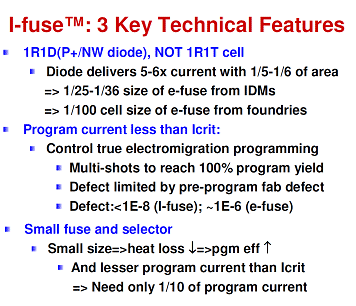
Fig. 2 Three key technical features of I-fuse™
OTP Applications
OTP allows each chip to be customized after fabrication to fix defects, adjust parameters, trim statistical variations, store permanent data, or personalize configurations. OTP can be used in chip IDs, security keys, product features selection, memory redundancy, device trimming, parameter or configuration storage, and code memory for MCU, as shown in Fig. 1.
Every chip needs OTPs if they can be reliable, available, and affordable in any CMOS processes. However, today’s OTP technologies need cells customized for different CMOS derivatives (e.g. LP, G, GP, HS), variations (e.g. logic, Mixed Signal, HV, BCD, CIS) or optical shrinks (10% or 15% shrink) even for those in the same generations from the same foundries. Porting between process generations and foundries has been very difficult and requires a long development time.
I-Fuse™ OTP: The OTP of Choice
I-fuse™ is a fuse-based OTP technology that uses (a) 1R1T cell to reduce cell size to 1/100, (b) limited program current below a catastrophic break point to increase reliability by 100x, and (c) small cell size to increase program efficiency to achieve 1/10 program current, comparing with the popular electrical fuse (e-fuse). The three key technical features are shown in Fig. 2 and further discussed as follows:
(1) 1R1D (P+/NW diode) vs. conventional 1R1T OTP cell
The I-fuse™ cell uses 1R1D (1 Resistor and 1 junction Diode), instead of 1R1T (1 Resistor and 1 Transistor) used in conventional e-fuse cells. Under the same voltage, a diode can deliver 5-6x more current in 1/5-1/6 of area compared with MOS. Therefore, the I-fuse™ has only 1/25-1/36 cell size of e-fuse cells from IDMs and 1/100 of those cells from foundries. The top view of an e-fuse and I-fuse™ cells are shown as in Fig. 3(a) and 3(b), respectively.

Fig. 3(a) Conventional 1R1T e-Fuse cell
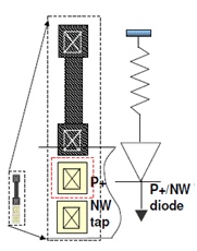
Fig. 3(b) 1R1D I-Fuse cell (illustration only)
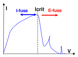
Fig. 3(c) Typical fuse I-V curve
(2) Program current below a catastrophic critical current, Icrit
A typical I-V characteristic of programming a fuse is shown in Fig. 3(c). When an applied voltage is high enough, the fuse can be heated up so that the fuse resistance is higher until a break point such that fuse suddenly breaks due to rupture, decomposition, or melt---which is the conventional way of programming a fuse.
On the contrary, programming of an I-fuse™ is to set current below Icrit to increase fuse resistance gradually without breaking the fuse. The I-fuse™ can be programmed in multiple shots until a satisfactory high resistance is reached. Program yield of an I-fuse™ is practically 100% such that the yield is determined by pre-programmed fab defects. In the past 3 years, we found only a few pre-program defects in more than 1 billion I-fuse™ accumulated from more than 30 silicon shuttles in 0.35um to 28nm CMOS. The I-fuse defect is less than 10-8, while an e-fuse defect is about 10-5 [1]. I-fuse™ achieves at least100x reliability over the conventional e-fuse.
(3) Small fuse and program selector
I-fuse™ cells are kept small to conserve heat so that temperature can be raised higher and faster to accelerate programming. Along with lowering the program current below Icrit, the I-fuse™ program current requires only 1/10 of a conventional e-fuse in the same CMOS technology, i.e. 7.5mA at 0.18µm for I-fuse™ and 18mA at 90nm for e-fuse after scaling width for current density comparision.
The I-fuse™ has been proven in silicon from 0.35µm to 28nm. The cell size and program current are scalable according to Moore’s law. I-fuse™ technologies can be continuously scaled to 16, 10nm and beyond.
OTP Merit Comparisons
Only a handful of OTP programming mechanisms are available, such as breaking fuse, breaking gate oxide, or storing charges, to create a permanent data state:
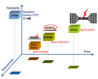
Fig. 4: OTP feature of merits
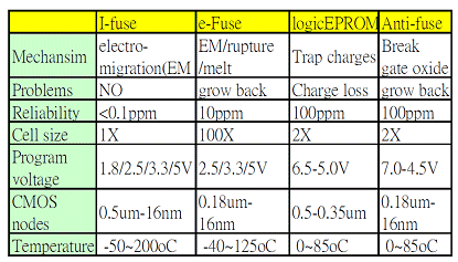
Table 1: feature comparison
(1) I-fuse™
I-fuse™ program mechanism is based on true electromigration (EM) that is the most reliable and most robust mechanism amongst all OTP technologies. I-fuse™ cell has only one fuse and one diode that is about half of an SRAM cell. The diode and fuse are two-terminal passive devices that are available and scalable in all CMOS technologies. The program voltages are very low that can meet the convenient I/O voltages of 1.8/2.5/3.3/5V for different CMOS generations. The temperature range is very wide from -50°C to 200°C, because the fuse does not suffer catastrophic damage during programming.
(2) Electrical fuse (e-fuse)
Electrical fuse with a 1R1T (1 Resistor and 1 Transistor) cell is the most popular OTP technology. However, the cell size is huge because of large MOS device. Programming an e-fuse is more like an explosion such that debris may micro-bridge to create shorts after prolong use or burn-in. The defect rate is about 10ppm (10 parts per million) [1].
(2) Logic EPROM (Electrical Programmable Read-Only Memory).
This OTP technology is based on storing charges in a floating gate to create “permanent” data state. However, the gate oxide must not be too thick for charge injection and too thin for data retention. The suitable gate oxide of 80Å happens for 0.35µm MOS devices, which means that 0.35µm or 0.5µm CMOS is the natural process for this OTP technology. Data retention limits the reliability to only 100ppm level and is sensitive to process variations.
(3) Gate-oxide breakdown Anti-fuse (AF)
AF is another OTP technology to create a “permanent” data state by breaking a gate oxide in a MOS device. Unfortunately, there is a “soft breakdown” mechanism associated such that broken oxide may appear to heal itself [2][3]. The thinner the gate oxide, the more severe the soft breakdown is. This OTP technology needs heavy redundancy to make the IPs work.
I-Fuse™: Reliability
I-fuse™ IP has been qualified by JEDEC JESD22-A108 (HTOL at 125oC for 1,000 hours) and JESD22-A103G (HTS at 300oC for 1,000 hours) in various foundries. Passing HTS at 300oC for 1,000 hours is unprecedented for any OTP technologies. The cell current variations are further measured for comparison before and after 1,000hr HTOL and HTS. The current changes are less than 2% as shown in Fig. 4(a) and 4(b). Specifically, I-fuse™ can pass 8 hours at 400°C with 0 defect in 3Mb, while a foundry e-fuse can not even pass 400°C for 2 hours with 20-30 defects in 1Mb. Redistribution Layer (RDL) applications require a die sustaining 2 hours at 400°C for interposer in 3D ICs.

Fig. 4(a) Cell current variations of 1Mb I-fuse™ at 0.18µm CMOS before and after 1,000hr HTS
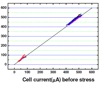
Fig. 4(b) Cell current variations of 1Mb I-fuse™ at 55nmLP CMOS before and after 1,000hr HTOL
A study was published in 2005 [4] discussing after burn-in behaviors of silicided polysilicon fuses under typical, under-programming, and over-programming that result in after burn-in resistance staying the same, increasing, or decreasing, respectively. The I-fuse™ behavior likes a typical programming so that the fuse resistance stays almost the same. However, the conventional e-fuse tends to have its resistance reduced after burn-in, which shows over-programming behavior. Resistance reduced after burn-in makes sensing window smaller that can cause the IP to fail.
Conclusion
I-fuse™ is a dream OTP comes true that combines the best of all OTP technologies has to offer: high yield, high reliability, high speed, high data security, high scalability, small size, easy-of-use, standard I/O voltages for programming, and wide temperature from -50°C to 200°C. I-fuse™ is also a universal OTP that has been proven from 0.5µm to 28/20/16nm in various CMOS derivatives, variations, half-nodes, and foundries.
Reference:
[1] G. Uhlmann, et al, IEEE ISSCC, Feb., 2008, pp 406-407.
[2] N. Klein, IEEE Trans. Elec. Dev., Vol. 13, No. 11, Nov., 1966, pp. 788.
[3] B.E. Weir, et al, IEEE IEDM, Dec., 1997, pp. 73-76.
[4] J. Fellnar, et al, IEEE IRPS, 2005, pp 446-449.
Related Semiconductor IP
- OTP
- Secure OTP
- 64x1 Bits OTP (One-Time Programmable) IP, TSMC 0.18um SiGe BiCMOS 1.8V/3.3V General Purpose Process
- 8Kx16 Bits OTP (One-Time Programmable) IP, DB HiTek AN180 1.8V / 5V Process
- 8Kx8 Bits OTP (One-Time Programmable) IP, MXIC 0.18um 1.8V/5V Logic/BCD Process
Related White Papers
- I-fuse: Most Reliable and Fully Testable OTP
- The Benefits of a Multi-Protocol PMA
- Last-Time Buy Notifications For Your ASICs? How To Make the Most of It
- The Growing Imperative Of Hardware Security Assurance In IP And SoC Design
Latest White Papers
- Ramping Up Open-Source RISC-V Cores: Assessing the Energy Efficiency of Superscalar, Out-of-Order Execution
- Transition Fixes in 3nm Multi-Voltage SoC Design
- CXL Topology-Aware and Expander-Driven Prefetching: Unlocking SSD Performance
- Breaking the Memory Bandwidth Boundary. GDDR7 IP Design Challenges & Solutions
- Automating NoC Design to Tackle Rising SoC Complexity