Optimal OTP for Advanced Node and Emerging Applications
By Joey Lee, eMemory
Advancements in semiconductor manufacturing have led to significant technological leaps with increasing demands for smart devices, 5G, EVs, metaverse, and generative AI. All these applications are driven by high-performance computing (HPC) capabilities, relying heavily on advanced process technology. While leading foundries keep pushing Moore’s law to the limit of physics, embedded non-volatile memory (eNVM) is becoming a game-changer in designing advanced integrated chips. As the world’s leading and largest pure-play eNVM IP provider, eMemory’s security-enhanced version of One-Time Programmable (OTP), NeoFuse, has achieved qualification on the TSMC N4P and N5A process, and more projects (e.g. N3P) underway for HPC and automotive applications. In this article, we will introduce the advantages of NeoFuse OTP on the TSMC advanced node platforms and how to leverage these advantages in the advanced processes.

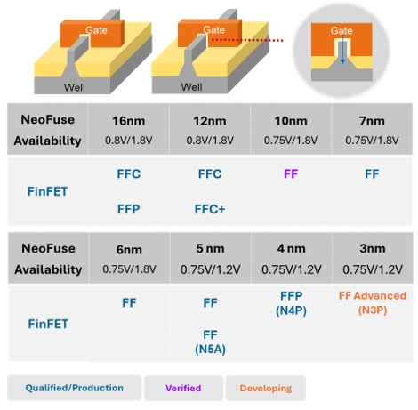
Figure 1. NeoFuse/NeoPUF Roadmap in Advanced Nodes
Empowering Diverse Applications with Robust Specifications
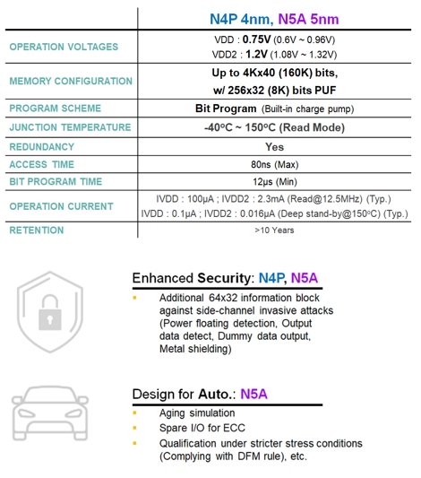
eMemory’s security-enhanced OTP, NeoFuse, boasts OTP and PUF array, bit-programming scheme, high-temperature tolerance (-40oC to 150oC), and enhanced security features to prevent side-channel and invasive attacks. For the N5A process specializing in automotive applications, more powerful features including full-redundancy, aging simulation, spare I/O for ECC are incorporated into the IP design to fulfill stringent qualification conditions and for higher reliability. For more detailed specifications, please refer to Figure 2.

Figure 2. NeoFuse/NeoPUF IP Features on N4P and N5A
With the advantages of the proprietary design, NeoFuse has demonstrated remarkable reliability and flexibility by achieving first-cut success in the N4P qualification processes.
Optimizing Design with Proprietary “In-Cell Voltage Divider”
In advanced FinFET platforms like N5 and N4, many challenges come along. As the gate insulators become thinner in advanced processes, it’s getting more difficult for the charge pump (CP) circuit to endure similar voltages as before for cell programming. Therefore, for better reliability, the size of the transistors in the CP circuits will inevitably become larger, making the IP peripherals bulkier. The difficulty in designing the CP circuit further increases with other side effects like GIDL current and punch-through effect.
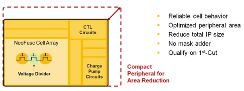
eMemory’s NeoFuse IP features a distinctive and proprietary “voltage divider” in the memory cell. The in-cell voltage divider greatly mitigates GIDL current and punch-through effect in high-voltage programming, alleviating the complexity of the charge pump circuit design. With the in-cell voltage divider, a more compact and optimized peripheral circuit design is easily achieved, which makes NeoFuse the best IP solution in terms of size and overall performance among all the other eNVM solutions.

Figure 3. NeoFuse Proprietary Architecture
Leveraging Inherent Advantages
NeoFuse has an unmatched track record as the first OTP technology to go into mass production at 7nm and below. With the inherent advantages of anti-fuse technology, eMemory’s NeoFuse OTP improves many aspects of the traditional eFuse technology in advanced FinFET platforms. For example, eMemory’s NeoFuse OTP boasts a smaller IP area. The advantages of anti-fuse OTPs increase as density grows. Given the trend of using higher density in advanced applications, this characteristic enables designers to achieve performance and yield effortlessly. In addition, NeoFuse offers higher reliability as its electronic characteristics stay unchanged even after unlimited times of read operations. For security requirements, the programmed status of NeoFuse is invisible, which is ideal for enhancing chip security. Last but not least, NeoFuse features an easier peripheral design for programming.
Conclusion
NeoFuse's higher reliability makes it a better choice for automotive, SRAM repair functions, and other advanced applications. Furthermore, NeoFuse offers greater extendibility and can be utilized with PUF-based solutions to meet the increasing demand for security in IoT applications. To learn more about eMemory’s NeoFuse, click here.
About eMemory
eMemory (TPEX:3529) is a leading pure-play developer and provider of logic-based Non-Volatile Memory (Logic NVM) founded in 2000, and since 2019, eMemory started to offer PUF-based Security IP solutions based on its outstanding anti-fuse and physical unclonable function (PUF) technology.
Following the breakthrough success of one-time programmable memories (NeoBit/NeoFuse), eMemory expanded its portfolio of IPs, including multi-time programmable memories (NeoMTP/NeoEE), Flash memories (NeoFlash/RRAM/MRAM), and PUF technology (NeoPUF). Additionally, with the subsidiary, PUFsecurity Corp., eMemory enters the security sector by offering innovative PUF-based security subsystems and solutions, such as Root of Trust Module PUFrt and Crypto Coprocessor PUFcc.
As a world-leading IP provider, eMemory has delivered best-in-class designs to over 2,400 foundries, IDMs and fabless companies globally, and commits to push the technology envelope together with our partners in advanced applications.
For more information about eMemory, please visit www.ememory.com.tw
Related Semiconductor IP
- OTP
- Secure OTP
- 64x1 Bits OTP (One-Time Programmable) IP, TSMC 0.18um SiGe BiCMOS 1.8V/3.3V General Purpose Process
- 8Kx16 Bits OTP (One-Time Programmable) IP, DB HiTek AN180 1.8V / 5V Process
- 8Kx8 Bits OTP (One-Time Programmable) IP, MXIC 0.18um 1.8V/5V Logic/BCD Process
Related White Papers
- Selection of FPGAs and GPUs for AI Based Applications
- Generative AI for Analog Integrated Circuit Design: Methodologies and Applications
- e-GPU: An Open-Source and Configurable RISC-V Graphic Processing Unit for TinyAI Applications
- Boosting RISC-V SoC performance for AI and ML applications
Latest White Papers
- Ramping Up Open-Source RISC-V Cores: Assessing the Energy Efficiency of Superscalar, Out-of-Order Execution
- Transition Fixes in 3nm Multi-Voltage SoC Design
- CXL Topology-Aware and Expander-Driven Prefetching: Unlocking SSD Performance
- Breaking the Memory Bandwidth Boundary. GDDR7 IP Design Challenges & Solutions
- Automating NoC Design to Tackle Rising SoC Complexity