Enabling Rapid Adoption of the AMBA 3 AXI Protocol-based Design with Synopsys DesignWare IP
Mick Posner, Synopsys, Inc
Portland, Oregon USA
Abstract:
To successfully develop an AMBA™ 3 AXI™ protocol-based design in the shortest amount of time possible requires more than just raw design expertise and individual, piecemeal IP components. It requires a comprehensive set of synthesizable IP, verification IP and an automated method to assemble the entire system-on-chip (SoC) subsystem.
The AMBA 3 Advanced eXtensible Interface (AXI) protocol builds on the many benefits of the AMBA 2.0 standard by greatly extending the performance and flexibility of the on-chip bus standard. But with this flexibility comes complexity. The DesignWare® IP solution for the AMBA 3 AXI protocol enables designers to quickly and easily integrate the high-speed protocol into their (SoC) designs, while reducing risk and speeding time to results. The DesignWare IP solution for the AMBA 3 AXI protocol provides access to three main required components including synthesizable IP, verification IP and automated subsystem assembly using the Synopsys® coreAssembler tool. The combination of these three offerings enable designers to substantially reduce the time spent in the design and validation of next generation high speed designs based on the AMBA 3 AXI protocol.
Technical Backgrounder—The AMBA 3 AXI Protocol
To correctly grasp the complexity of the design challenge facing an engineer of an AMBA 3 AXI protocolbased design, we must first understand the technical features of the AMBA 3 AXI protocol itself. The AMBA 3 AXI protocol was developed to address the needs of next generation designs and was created in collaboration with more than 30 companies, one of which is Synopsys. The AMBA 3 AXI protocol defines a unidirectional channel architecture, which enables the efficient use of register slices to pipeline the connection for higher speeds. The support of multiple outstanding transactions and out-of-order transaction completion, coupled with the efficient use of the read, write and address/control channels, enable systems to achieve levels of performance and efficiency. This performance is limited only by the capabilities of the peripherals themselves.
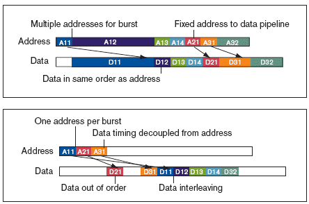
Fig 1: The technical advantage of the AMBA 3 AXI protocol over AMBA 2.0 AHB.
The AMBA 3 AXI Protocol: Channel Power
The AMBA 3 AXI architecture differs significantly from previous AMBA protocols with the introduction of channels. Each of the five independent channels consists of a set of information signals and uses a two-way VALID and READY handshake mechanism. The information source uses the VALID signal to show when valid data or control information is available on the channel. The destination uses the READY signal to show when it can accept the data. Both the read data channel and the write data channel also include a LAST signal to indicate when the transfer of the final data item within a transaction takes place. Read and write transactions each have their own address channel. The appropriate address channel carries all of the required address and control information for a transaction. The Read data channel conveys both the read data and any read response information from the slave back to the master. The Read data channel includes the data bus, which can be 8, 16, 32, 64, 128, 256, 512, or 1024 bits wide and a read response indicating the completion status of the read transaction. The Write data channel conveys the write data from the master to the slave. The Write data channel includes the data bus, which can be 8, 16, 32, 64, 128, 256, 512, or 1024 bits wide, and one byte lane strobe for every eight data bits, which indicates which bytes of the data bus are valid. The unaligned transfer support makes for a more efficient use of the bus yielding higher performance, lower latency and increased bandwidth operation.
DesignWare IP Solutions for AMBA 3 AXI
With the complexity of the AMBA 3 AXI protocol the task of designing and verifying a subsystem based on this standard becomes a major undertaking, requiring a vast amount of expertise. The DesignWare IP solutions for AMBA 3 AXI are designed to ease this design task by providing engineers access to the common design and verification IP blocks, which enable rapid implementation and validation from the block to subsystem level. In addition, the coreAssembler tool automates the assembly of the subsystem and testbench infrastructure. Designers are able to rapidly assemble, synthesize and verify AMBA 3 AXI based designs when using the DesignWare solutions for AMBA 3 AXI.
DesignWare Synthesizable IP for AMBA 3 AXI
The DesignWare synthesizable IP is the first part of the three part solution, which enables rapid adoption of high bandwidth, low latency, and high performance AMBA 3 AXI protocol-based designs. The synthesizable IP includes three key elements: the interconnect bus fabric, an AXI-to-AHB slave bridge, and master and slave generic interface modules. These components are the fundamental building blocks of any new SoC and enable designers to easily implement the AMBA 3 AXI protocol based architecture. These IP components also help transition existing IP and application specific blocks to AMBA 3 AXI, thus ensuring high reuse productivity.
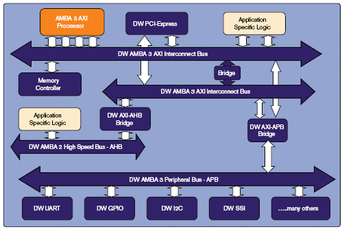
Fig 2 – DesignWare Synthesizable IP for AMBA 3 AXI and AMBA 2.0 AHB/APB.
The DesignWare Interconnect Fabric for AMBA 3 AXI, (DW_axi) has a set of features that make it by far, the best solution for a standardized interconnect fabric for AMBA 3 AXI protocol-based design. The configuration flexibility of the DW_axi provides engineers with a feature set that matches their prioritized design requirements. The DW_axi is an RTL interconnect implementation of the AMBA 3 AXI protocol, where simultaneous transfers between different masters and slaves can occur. The component can be configured to support up to 16 masters and 16 slaves supporting all protocol specified address and data widths. The DW_axi is based on a multiple address, multiple data bus architecture with an optional built in system decoder. Every transaction has address and control information on the address channel that describes the nature of the data to be transferred. The data is transferred between master and slave using a write data channel to the slave or a read data channel to the master. In write transactions, in which all the data flows from the master to the slave, the AMBA 3 AXI protocol has an additional write response channel to allow the slave to signal to the master the completion of the write transaction. This multi-layer interconnect architecture allows parallel traffic between different master/slave pairs on all five AMBA 3 AXI channels. Therefore, system bandwidth is not limited by the DW_axi but by the external master and slaves.
In addition to offering combinatorial built address and data channel control, the DW_axi enables the highest possible operational frequency, bandwidth and performance by providing the feature of internal and external pipelining, known as register slicing. The configurable internal and external register slices can be applied to individual channels on either the full path or just the forward control path providing the maximum of flexibility to timing options and yielding optimal performance. To optimize the DW_axi for optimal performance and guarantee minimum area, it includes a slave visibility feature, which is used when not all slaves are visible to all masters. This customizes the visibility of master access to each slave for both normal and boot modes and results in the reduction in complexity of the arbitration logic. This enables optimal performance to be achieved with the minimum of logic.
One of the key goals of the AMBA 3 AXI protocol is interoperability with the existing AMBA 2.0 technology. To enable this interoperability the DesignWare IP solution includes an AMBA 3 AXI bridge to AMBA 2.0 AHB, (DW_axi_x2h). The DW_axi_x2h provides support for connection to a complete AMBA 2.0 AHBbased subsystem providing reuse support for an existing AHB based subsystem. In “Lite” mode standalone slave components can be connected directly to the AMBA 3 AXI protocol based bus. A clear advantage of this interoperability is that designers have access to a wide array of existing DesignWare silicon-proven, synthesizable and verification IP for the AMBA 2.0 AHB and APB protocols. This increases the options for reuse and again increases the time designers spend on design differentiation rather than general subsystem creation and validation. The DesignWare synthesizable IP solution includes other common AMBA 2.0 based design blocks such as the AHB bus fabric, DW_ahb, APB Bridge and fabric, DW_apb, and many peripheral blocks such as DMA, memory controller, I2C, SSI, GPIO, RTC, Timers and interrupt controllers.
Another set of the reusable infrastructure components that ease the adoption of AMBA 3 AXI protocolbased designs are the DesignWare generic interface modules for master and slaves, DW_axi_gm/gs. The DW_axi_gm/gs uses a generic interface, which reduces the complexity required to port a custom IP or specific applications to the AMBA 3 AXI protocol-based bus. When connecting the custom application or IP to the AMBA 3 AXI protocol- based bus, the designer does not have to worry about the protocol specifics because the DW_axi/gs modules handle most of the AMBA 3 AXI interface specifics. Using the generic interface modules frees up designers time to focus their skills on proof checking the applications operation after it has been connected to the AMBA 3 AXI bus.
DesignWare Verification IP for AMBA 3 AXI
The second part of the DesignWare IP solution which enables rapid adoption of AMBA 3 AXI protocol based design is the Synopsys DesignWare Verification IP (VIP) for AMBA 3 AXI. This verification IP provides a quick and efficient way to verify AMBA 3 AXI-based SoC designs by bringing advanced techniques for more productive verification to the fingertips of the verification engineers. The DesignWare Verification IP for AMBA 3 AXI includes the following components: Master, Slave, Monitor and verification interconnect. Each component supports all the AMBA 3 AXI address and data widths in addition to all protocol transfer and response types. The master and slave VIP’s are used to generate and respond to transactions. The verification interconnect enables the creation of a full interconnected functional subsystem to aid testing during block level integration of multiple block interactions. The verification IP includes a full-featured command set, which enables directed transaction, level command-based testing. The verification IP will quickly flush out interconnection errors, functional bugs and hit many corner cases.
The verification IP has received the AMBA 3 Assured logo certification. This logo indicates that the DesignWare Verification IP has been proven to correctly implement the AMBA 3 AXI specification, as defined by the assertion-based AXI protocol rule sets from ARM. When the verification IP is used at the block level, the engineer is assured that the blocks’ interface will be tested to conform to the AMBA 3 AXI protocol specification. This eases the block-level integration into the final subsystem because the engineer has already proven that it is AMBA 3 AXI-ready. The DesignWare verification IP can also be used at the subsystem level to exhaustively test the master/slave block interaction as well as creating realistic application traffic. While doing this, the engineer knows that the AMBA 3 Assured DesignWare verification IP is ensuring that the AMBA 3 AXI protocol specification is not being violated.
DesignWare Verification IP and the Reference Verification Methodology
The DesignWare Verification IP supports a reusable layered, coverage driven, constrained random verification methodology, which can be used to quickly generate thousands of transactions. The constrained random verification generation is defined by the Synopsys Reference Verification Methodology (RVM). RVM is an implementation of the best practices documented in the Verification Methodology Manual which is available now. This methodology defines a powerful method for automatically generating transactions to stress the maximum number of protocol combinations. The constrained-random, coverage-driven methodology provides higher productivity and quality verification for large, complex designs compared to the traditional directed-test methodology. In the directed-test approach, engineers write individual tests to verify specific design features. This process can be very time consuming, especially for complex devices with large numbers of interacting features. So time consuming, in fact, that often designs must be taped out prior to reaching the verification quality target, leading to an increased chance for an expensive silicon re spin.
With a constrained-random, coverage driven approach, engineers write high-level constraints that describe realistic input scenarios for the design. The advanced verification tools and verification IP will use these constraints to automatically generate many thousands of tests–even tests that the engineer didn’t think of–to verify the design. Functional coverage is used to guide verification and measure progress. The result is that verification quality targets can more easily be met prior to tape-out, even for the most complex designs. The Reference Verification Methodology that can be used to implement a constrained random verification environment is built on a reusable infrastructure, which enables tests at a block level to be reused at the block level, subsystem level and across multiple projects. RVM-driven verification IP means the designer writes a minimal number of tests, which in turn generates thousands of tests, fully stressing the block or subsystem with realistic bus traffic. The Synopsys RVM based environment provides a uniform interface to all verification components so the environment is easy to understand and can be quickly reused across other projects.
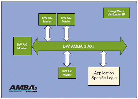
Fig 3: Block level verification using DesignWare verification IP for AMBA 3 AXI.
To accelerate the verification of an AMBA 3 AXI protocol base system, the DesignWare Verification IP should be used to verify individual component interfaces, employed at the subsystem, and then finally at the full system level. At the block level the verification IP is used to generate efficient and accurate stimuli to test the applications of the AMBA 3 AXI interface. The tests created at this level will be able to be re-run at the subsystem level if the tests are written according to the RVM guidelines. Since the DesignWare Verification IP for AMBA 3 AXI is “AMBA 3 Assured” certified, the designer has increased confidence in the quality of the verification process.
Efficient verification of an initial AMBA 3 AXI based subsystem is achieved by replacing a number of the loosely coupled IP and design blocks with the DesignWare Verification IP. This enables the interconnections, transactions and features to be quickly verified and a set of robust high coverage tests to be created. DesignWare Verification IP masters and slaves are used to replace the components and then the master VIP is used to create both directed and constrained random verification transactions. This method allows fast creation of subsystem stimuli and responses that will quickly flush out any design interconnection issues. The monitor in the DesignWare Verification IP is used to check the compliance to the AMBA specification and provide direct hooks for the testbench-based scoreboard.
Click to enlarge
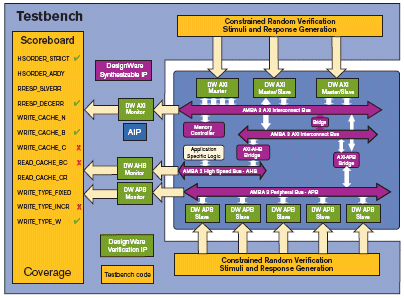
Fig 4: Building a Subsystem verification Environment using DesignWare Verification IP.
A scoreboard is essentially a block of testbench code which provides an automatic and intelligent way to track transactions, coverage and data flow. For data, it can be set up to track the source golden data and compare it with the destination data to create a pass fail criteria for the tested data path. The scoreboard is directly linked to the DesignWare Verification IP monitors enabling all transaction and coverage data to be extracted, captured and verified. One of the advantages of using the DesignWare Verification IP monitors is that the same scoreboard-based verification environment continues to function when the master and slave verification IP blocks are removed and replaced with the actual RTL for system level testing. When the monitors are passive components, they can be used throughout the verification cycle.
To further speed up the verification task, assertion IP should also be included into the block and subsystem level environment to enable the use of formal and hybrid formal verification tools such as the Synopsys Magellan™ tool. Both the verification IP and the assertion IP should be included in the verification environment. The verification IP monitor provides the advanced simulation features like cross-port coverage and scoreboard notification support. Since ARM supplies and defines the assertion IP as the executable specification, it can be used as the golden reference. All the DesignWare Verification IP components have been verified against the ARM supplied assertion IP as part of the “AMBA 3 Assured” certification process. In addition, the monitor in the DesignWare Verification IP helps determine when the verification is complete by tracking and logging each transaction, providing coverage information, and giving errors and warnings of protocol violations.
The final verification stage is full system level verification. At this stage the RTL for the loosely coupled application components and IP should be included. The external interfaces must also be verified and other DesignWare Verification IP can be employed at this point to reduce the effort of the system level testing. Designers can use a broad portfolio of DesignWare Verification IP, which are included as part of the VCS® Verification Library and the DesignWare Library products including, PCI Express®, Serial IO, I2C, Ethernet, USB, USB-OTG and thousands of device based memory models. The DesignWare Verification IP master for AMBA 3 AXI should still be used to generate the stimuli as the original subsystem tests can be immediately reused. Other DesignWare Verification IP can also be tied directly into the scoreboard, providing a closedloop intelligent verification platform.
Click to enlarge
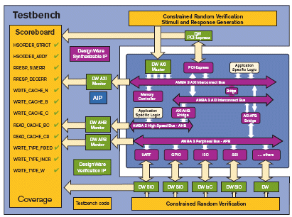
Fig 5: System Level Verification with DesignWare Verification IP.
The verification engineer also wants to simulate the design, testbench, verification IP, assertion IP as quickly as possible. This high performance simulation is achieved when the Synopsys VCS simulator is used. VCS optimizes the complete design environment, design, testbench, verification IP and assertion IP into a single unified kernel. This single compiled kernel removes the communication and synchronization overhead that is found in traditional simulation environments. This method gains the designer 5X or more simulation performance. To the verification engineer, this means that regressions that previously ran for say five days, is now complete in less than one. This frees up engineering time to run additional validation to increase coverage numbers, and in turn increase the confidence in the end design.
Bringing it all together: DesignWare IP with Synopsys’ coreAssembler Tool
The third part of the DesignWare IP solution, which enables rapid adoption of AMBA 3 AXI protocol based design is the Synopsys coreAssembler tool. When the DesignWare Library IP is used with the coreAssembler tool, it enables the designer to automatically assemble simulate and synthesize AMBA-based subsystems in less time than ever before. The coreAssembler tool automates the subsystem design creation and block integration of both AMBA 3 AXI, and AMBA 2.0 AHB/APB components. The coreAssembler tool reduces the time spent creating application specific subsystems that include DesignWare IP. This again, allows the designer to focus on additional product testing or differentiation. The coreAssembler tool fully supports the “Structure for Packaging, Integrating and Re-Using IP Within Tool-Flows”, SPIRIT, format, so 3rd party and custom IP blocks, which are SPIRIT-compliant can be packaged effortlessly into the assembled subsystem.
The DesignWare synthesizable and verification IP is packaged with “assembly intent”. This is the built in,protocol-specific expertise that enables the coreAssembler tool to automatically connect, or wire the IP blocks to each other. The Synopsys assembly expertise comes from many years of real life AMBA IP and AMBA-based subsystem creation. Any AMBA 3 AXI or AMBA 2.0 single or multi-layer subsystem configuration is supported, in addition to AMBALite configurations. For example, if the designer includes the AMBA 3 AXI interconnect fabric, and the AMBA 3 AXI bridge to AMBA 2 AHB components, the built in assembly knowledge within the coreAssembler tool enables automatic connection of the two AMBA 3 AXI interfaces together. This correct by construction automation removes the chance of typo created wiring errors All DesignWare Library synthesizable IP components are packaged with this design expertise and a set of default parameters. Therefore, creating an initial subsystem design is as easy as a couple of clicks, pull down menu selections and a couple of subsystem level configuration parameter option confirmations.
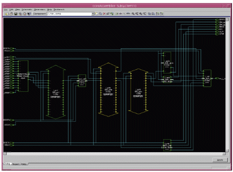
Fig 6: Screen shot of an AMBA 3 AXI based design within coreAssembler.
The coreAssembler tool helps avoid multiple IP miss-configurations by supporting a hierarchical design approach with cross propagation of design parameters and system level parameters. The parameters, such as address and data widths can be locked at the top level and propagated to the lower level IP blocks ensuring IP miss-configurations are avoided. This automation and built in parameter checking eliminates the chance of IP configuration errors, which can lead to lengthy subsystem debugging. Remember the quicker the engineer can get the first subsystem simulation up and running, the more time the verification engineer will have to verify the operation of the subsystems specific application.
To achieve optimal synthesis results, the coreAssembler tool automates the running of the Synopsys synthesis tools including Physical Compiler® and Design Compiler®. Designers can choose from multiple synthesis methodologies, such as area_timing, timing_area, ACS and low power optimized flows. User defined flows can also be created and included into the coreAssembler automated flow.
To help reduce the time to first simulation, the coreAssembler tool automatically creates a verification infrastructure that includes DesignWare Verification IP specifically targeting the assembled subsystem. In addition to the creation of the infrastructure, the tool also generates stimuli for the DesignWare Verification IP to ping test the subsystem. Currently these are simple pings tests that write to an IP component register, and then read it back to ensure the contents were correctly written. While this seems easy to do, it is actually the first milestone of many subsystem designs and with traditional subsystem development, could have taken weeks to achieve. With the DesignWare Library IP and coreAssembler flow, this subsystem ping test can be achieved within a matter of hours.
The automated flow also makes late engineering changes incredibly easy to handle. For example, let’s say that the subsystem was designed with a 32 bit data bus and the chief architect decides at the last minute that a 64 bit data bus is going to be needed to achieve the target performance. In a traditional design flow, the engineer would have to re-configure and modify many RTL files, which on its own would take a lot of time and could introduce typo or incorrect connection errors. With the coreAssembler flow, the change can be completed with a simple modification to a top level parameter, which will then be propagated automatically down to the lower level blocks. The new RTL code will be automatically re-created along with new testbench infrastructure files.
Summary
The main barriers to adopting an AMBA 3 AXI protocol-based design for high performance SoCs is the availability of synthesizable IP, verification IP and the ability to efficiently create complex architectures in the shortest time as possible. To meet the demanding market window constraints, all these parts must be readily available to the design engineer. With the Synopsys DesignWare Library and coreAssembler tool these three crucial parts are made available. The DesignWare synthesizable IP for AMBA 3 AXI and AMBA 2.0 AHB/APB contain the required infrastructure building blocks for most next generation subsystems. The DesignWare Verification IP for AMBA 3 AXI and AMBA 2.0 AHB/APB meets and exceeds the requirements created by the verification challenges of a complex high performance subsystem. Finally the Synopsys coreAssembler tool brings the synthesizable and verification components into an automated flow optimizing the creation, simulation and synthesis of the subsystem design. The DesignWare IP solutions for AMBA eases the adoption of AMBA 3 AXI protocol based design.
For more information on Synopsys DesignWare IP, visit www.synopsys.com/designware.
Related Semiconductor IP
- ReRAM NVM in DB HiTek 130nm BCD
- UFS 5.0 Host Controller IP
- PDM Receiver/PDM-to-PCM Converter
- Voltage and Temperature Sensor with integrated ADC - GlobalFoundries® 22FDX®
- 8MHz / 40MHz Pierce Oscillator - X-FAB XT018-0.18µm
Related Articles
- Designing Using the AMBA (TM) 3 AXI (TM) Protocol -- Easing the Design Challenges and Putting the Verification Task on a Fast Track to Success
- Context Based Clock Gating Technique For Low Power Designs of IoT Applications - A DesignWare IP Case Study
- PCIe IP With Enhanced Security For The Automotive Market
- The Growing Imperative Of Hardware Security Assurance In IP And SoC Design
Latest Articles
- An FPGA-Based SoC Architecture with a RISC-V Controller for Energy-Efficient Temporal-Coding Spiking Neural Networks
- Enabling RISC-V Vector Code Generation in MLIR through Custom xDSL Lowerings
- A Scalable Open-Source QEC System with Sub-Microsecond Decoding-Feedback Latency
- SNAP-V: A RISC-V SoC with Configurable Neuromorphic Acceleration for Small-Scale Spiking Neural Networks
- An FPGA Implementation of Displacement Vector Search for Intra Pattern Copy in JPEG XS