Can the chip design - verification divide be plugged in with some knee jerk band aid type strategies?
By Sunil Kakkar, VP of Engineering Operations, MosChip Semiconductor
Not if we are open to facing the fact that “completing functional verification” has become one of the most critical requirement of handing off the chip design to the fab and the continuous survey inputs are reinforcing the truth that the multi million dollar problem is only getting worse every minute.
The unprecedented convergence of wireless and electronic devices requires the SOCs to have a microprocessor, DSPs, custom logic (digital & analog) and memory all on a single chip with a continuous need for ever growing functionality as well as performance improvements. The highest quality working silicon should be 100% functional and should hit the shelves on time.
If we all agree that the ever shrinking time to market and the very miniscule window for profitability of these extremely power packed complex SOC designs pose a serious crisis then why do we not want to approach the problem with a well defined strategy in mind.
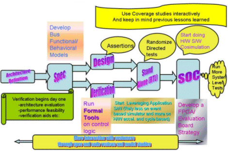
We read an article about the unsurpassed benefits of a functional formal verification tool and we are ready to throw out the traditional simulation based verification techniques in favor of advanced mathematical analysis techniques, not realizing that formal verification does not work well on data paths or on large pieces of control logic. A formal verification tool is most efficient when it is used for controlled surgical strikes on small pieces of most complex control logic like the ones in arbiters and cache coherency checkers. Even then, it takes a lot of skill and practice to meaningfully constrain the design when running these mathematical checks so that the formal engines can converge to a conclusion in a realistic framework of time. Formal verification should begin in the early stages of design and is not suited at all for chip level verification.
Similarly, Random Test Pattern Generation or RTPG as it is called can be an invaluable tool in getting to the corner case bugs in simulation, that cannot be imagined by the verification engineer, but is useful only if it is kept targeted or directed towards the functionality where we are wary of the existence of bugs. A lot of empty shots in the dark with the hope of getting a bug are as good as the chance of hunting success with the same strategy. A solid RTPG strategy also owes its success to a well thought out set of assertions that continuously check and monitor the design in the background for any design discrepancies while the random tests run in the foreground. Wise coverage metrics also help determine the convergence of the random test patterns with the functionality exercised with these random tests. We do not want to waste valuable simulation cycles on test patterns that do not exercise a piece of design logic that has not been covered in any other test.
Many of the verification strategies also fall flat on their face because no one wants to see the bigger picture. The individual module designers get so engrossed in the verification of their blocks that they do not visualize the fact that these blocks will eventually go into an SOC which will include blocks from other designers and even third party IP vendors. When so integrated, the verification strategy will have to have tests for checking out the intra block connections and timing. Each individual block’s logic at that time will also be subjected to hitherto unknown transactions and timing constraints. This is where a good chip level verification strategy comes in very handy.

What has to be continuously remembered is that every chip today, is being designed for a targeted family of devices that run a certain set of application programs which in turn expect the device to behave in a particular manner. These application program reviews can contribute to a solid system level verification strategy where these real life kind of testing is accomplished to evaluate how well the SOC will do out in the field.
Finally, all designs should be verified in a silicon kind of a situation, whether it is FPGA, hardware accelerated or an emulation solution. At that time, O/S kind of a code that will eventually be what the customer will see of the design must be run on the design to ensure that the design will do fine in the cool looking colorful device that is sold in the market.
It is this kind of a comprehensive and a complete verification strategy that begins with performance runs at the time of architecture development and ends up running the actual silicon on an evaluation board with the verification plan for each of the intermediate stages of design being well thought out, which can ensure that a bug free chip design does not remain a dream but it becomes a goal with a well defined plan.
Related Semiconductor IP
- UFS 5.0 Host Controller IP
- PDM Receiver/PDM-to-PCM Converter
- Voltage and Temperature Sensor with integrated ADC - GlobalFoundries® 22FDX®
- 8MHz / 40MHz Pierce Oscillator - X-FAB XT018-0.18µm
- UCIe RX Interface
Related Articles
- Differentiation Through the Chip Design and Verification Flow
- AI, and the Real Capacity Crisis in Chip Design
- The pivotal role power management IP plays in chip design
- David vs. Goliath: Can Small Models Win Big with Agentic AI in Hardware Design?
Latest Articles
- An FPGA-Based SoC Architecture with a RISC-V Controller for Energy-Efficient Temporal-Coding Spiking Neural Networks
- Enabling RISC-V Vector Code Generation in MLIR through Custom xDSL Lowerings
- A Scalable Open-Source QEC System with Sub-Microsecond Decoding-Feedback Latency
- SNAP-V: A RISC-V SoC with Configurable Neuromorphic Acceleration for Small-Scale Spiking Neural Networks
- An FPGA Implementation of Displacement Vector Search for Intra Pattern Copy in JPEG XS