Analogue synthesis for SoC
THE TREND TO INTEGRATE MORE ANALOGUE FUNCTIONS ON-CHIP DEMANDS A CHANGE IN ANALOGUE DESIGN TECHNIQUES, AWAY FROM MANUALLY INTENSIVE APPROACHES TO AUTOMATED SYNTHESIS
Over the past five years we have seen a consistent growth in the mixed-signal system-on-chip (SoC) market. Technical advances in integrated circuit (IC) manufacturing processes have made it possible for true electronic systems, such as cameras and radio systems, to be integrated on a single silicon substrate. This emerging market is predicted to have very high growth rates in the order of 40% over the next five years. In 2005, it is expected that 65% of all SoCs will contain some analogue components.
As seven out of ten complex chips will contain analogue, it means that there will be a fundamental shift from the way we currently design ICs to the way we will design ICs in a few years from now.
Unfortunately, while this demand for analogue has escalated, the supply has remained essentially flat, leading to a significant shortage. The number of analogue designers is not increasing and neither is their productivity, as they use basically the same methods and tools as they have for many years.
There are several reasons that make analogue circuit design in an SoC a very complex task. First, analogue circuit performance depends on the transistor behaviour. Small variations in the manufacturing process can result in dramatic changes in circuit performance. This translates into a need for accurate transistor models over different process corners. Another important concern in mixedmode ICs is substrate noise coupling. Fast-switching digital circuitry can affect sensitive analogue signals. Also careful layout to reduce device mismatches and parasitics is crucial to guarantee correct circuit behavior.
DESIGN KNOWLEDGE
Further, the current design flow does not encapsulate the knowledge of the designer and, as such, it cannot be used later by a less experienced designer. For example, an experienced designer might know exactly what to tweak, change or be watchful of in a design. However, this information is not embedded anywhere so if that experienced engineer decides to leave the design group most of that information is lost.
The completely different design schedules of analogue and digital were not an issue when two separate parts were sold. Semiconductor companies would market a new chipset every time a new IC process was released, even though only the digital part had changed. Today, in order to take advantage of the new process technologies, semiconductor companies are forced to have comparable design schedules for both analogue and digital.
SYNTHESIS TOOLS
In order to reduce the design cycle time using the above mentioned approach, several commercial tools for the automation of the analogue design process have become available on the market. These tools are best suited for design centering of circuit blocks. They are designed to increase the productivity of an already experienced circuit designer.
One technique is simulation-based analogue synthesis. It uses a loop-based structure. The loop comprises an optimiser proposing a candidate circuit and the evaluation engine, evaluating the quality of each candidate. This keeps looping until the specification is met. The commercially available tools use Spice and a numerical search engine or a bunch of numerical search engines. The method is CPU intensive and it is virtually impossible to handle a circuit with more than a few tens of transistors.
An alternative is to use more direct mathematical techniques. Both transistor behaviour and performance measures for analogue IP blocks, such as PLLs and data converters, can be formulated as posynomial functions of the design variables. These design problems can then be formulated as geometric programs, a special type of convex optimisation problem for which very efficient global optimisation methods have recently been developed. The synthesis method determines the globally optimal design.
Because PLLs take a long time to design, are very prone to errors and extremely sensitive to noise, the typical solution is to build and test one or two PLLs that cover as many different applications as possible. When one works, and this is usually after one or two silicon re-spins, the same PLL, after a few tweaks, is used. However, this leads to sub-optimal designs and, more importantly, as frequencies get higher and the jitter/noise rejection requirements become more challenging, this becomes less of a viable option.
The principle behind analogue synthesis is that once all the design know-how has been captured the user can define his PLL requirements, specify target process and circuit parameters such as input frequency and frequency multiplication factors, specifications on area, power, clock jitter and so on.
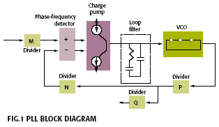
Miró is a PLL engine devised by Barcelona Design and Figure 1 shows the topology of the basic PLL structure that it uses. The PLL assumes that a stable reference frequency will be provided and this will typically be multiplied up to some higher frequency to be used on-chip. The phase-frequency detector (PFD) is based on a D-type flip-flop circuit that can detect the lead or lag of the phases and frequencies. A reset delay is used in the feedback path to remove the dead zone in the PFD/charge-pump transfer function.

RIPPLE AND NOISE
The charge pump uses a current steering technique and charge sharing when the transistors are switching, thereby reducing the jitter. Statistical variations between nominally matched devices in both the charge pump and the phase-frequency detector are taken into account in both the static phase error and jitter constraints. The loop filter is a second-order filter used to attenuate control-voltage ripple. The voltage controlled oscillator (VCO) is a single-ended current controlled oscillator controlled by a V-I converter. The VCO uses an amplifier in the V-I converter as an ‘active-cascode’ to improve the power supply rejection ratio. There are also internal decoupling capacitors to maximise the high-frequency power supply rejection.
The synthesis engine takes into account a large number of power-supply noise sources. These include sinusoidal noise sources added at the low frequencies (the crossover frequency), high frequencies, white noise, as well as steps on the power supply. The user can specify the amplitude of each of these different noise sources at the beginning of the optimisation process. The user then specifies maximum allowable peak jitter and cycle-to-cycle jitter due to these different sources. In this way, the user can ensure the PLL will operate according to specifications in a harsh, mixed-signal environment.
The output of the VCO drives a small swing to CMOS converter and is then usually divided by two to achieve a 50% output duty-cycle. If phase alignment with the on-chip clock is necessary, the user can insert a replica of their clock tree in the feedback path. The divider, if present, will employ a retiming latch to eliminate any jitter added by this block.
DESIGN INPUTS
The engine takes as user input all of the well-known top-level specifications of a PLL. Therefore, only an understanding of top-level specifications is required from the user. The process of mapping design specifications to component sizes, transistor widths and lengths and sizes of capacitors and resistors in the PLL is automated.
Geometric programming allows design constraints to be formulated hierarchically. The design constraints of the sub-blocks of the PLL – such as the charge pump and VCO – are formulated as functions of their input and output specifications. For example, the output current mismatch of the charge pump is formulated in posynomial form as a function of the transistor sizes and parameter values of the charge pump.
The threshold voltage mismatch is another important consideration. This mismatch is modeled as the variation between the threshold voltage for a particular transistor, and the nominal threshold voltage for the process is modeled as a random variable. The variance is inversely proportional to the area of the device. The standard deviation in the current is modeled as the percent variation between the saturation current for a particular transistor, and the nominal saturation current for the transistor in the process as a random variable with the variance set to be inversely proportional to the area of the device.

The system-level design constraints of the PLL are formulated in terms of the I/O specifications of the sub-blocks. For example, the contribution of the output current mismatch of the charge pump to PLL jitter is written in posynomial form. This hierarchical formulation results in a modular description for the geometric program. It results in better maintainability of the implementation and enables reuse of code when implementing the method for different PLL topologies. For example, if we want to use a different charge pump in the PLL only the much smaller charge pump module of the code needs to be updated.
The power for each sub-block is one of its I/O variables and can in turn be expressed as a posynomial function of its design variables. Another example is the stability condition for the PLL, and this can be obtained by deriving posynomial constraints on the phase margin and gain margin from the loop gain expression of the PLL.
To ensure high manufacturing yield, the IP needs to be optimised over multiple process corners. Supply- voltage variation and on-chip bias resistance variations are included as parameters. In addition to this, the user, by means of input parameters, has control over: the amount of noise seen by the PLL on the supply and substrate; the mismatch in transistor threshold voltage, and the mismatch in drain current.
On a 1.8V supply, the optimisation is designed to ensure that all the specifications are met at both 1.62 and 1.98V, that is Vdd ±10%. Although power consumption may be worst case at 1.98V, saturation margins will be worst case at 1.62V. The percent variation of any on-chip resistor also needs to be taken into account. If this value is 20%, the optimisation ensures that all the specifications are met with a resistance variation of ±20%. As resistors are used in the voltage reference and loop-filter circuits, and therefore critical to the manufacturing yield, both reference current variation and stability margins are taken into account during optimisation.
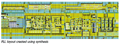
We have used Miró to synthesise a number of PLLs in 250, 180 and 130nm processes from both pure-play foundries and integrated device manufacturers. GDSII layouts have been submitted directly to the foundry without any changes. They demonstrate that synthesis based on geometric-programming techniques is viable for analogue blocks.
Navraj Nandra is director of worldwide applications for Barcelona Design
Related Semiconductor IP
- NPU IP Core for Mobile
- MSP7-32 MACsec IP core for FPGA or ASIC
- UHF RFID tag IP with 3.6kBit EEPROM and -18dBm sensitivity
- NPU IP Core for Edge
- Specialized Video Processing NPU IP
Related White Papers
- UPF Constraint coding for SoC - A Case Study
- Push-Button NoCs for SoCs
- Accelerating SoC Evolution With NoC Innovations Using NoC Tiling for AI and Machine Learning
- Early Interactive Short Isolation for Faster SoC Verification
Latest White Papers
- Ramping Up Open-Source RISC-V Cores: Assessing the Energy Efficiency of Superscalar, Out-of-Order Execution
- Transition Fixes in 3nm Multi-Voltage SoC Design
- CXL Topology-Aware and Expander-Driven Prefetching: Unlocking SSD Performance
- Breaking the Memory Bandwidth Boundary. GDDR7 IP Design Challenges & Solutions
- Automating NoC Design to Tackle Rising SoC Complexity