DDR5 IP
Filter
Compare
154
IP
from
24
vendors
(1
-
10)
-
DDR5 & DDR4 COMBO IO for memory controller PHY, 4800Mbps on TSMC 12nm
- The DDR5&DDR4 COMBO IO is used to transfer the Command/Address/Clk and Data between the memory controller PHY and the DRAM device
- The TX is designed to send information from PHY to DRAM and RX is designed to receive information which is from DRAM._x000D_ It supports DDR5&DDR4 interface
- The DDR5 DQ data rate can be up to 4800Mb/s, and the DDR4 DQ data rate can be up to 3200Mb/s and CA is SDR mode.
-
DDR5 MRDIMM PHY and Controller
- The DDR5 12.8Gbps MRDIMM Gen2 PHY and controller memory IP system solutions double the performance of DDR5 DRAM.
- The DDDR5 12.8Gbps design and architecture address the need for greater memory bandwidth to accommodate unprecedented AI processing demands in enterprise and data center applications, including AI in the cloud.
-
MRDIMM DDR5 & DDR5/4 PHY & Controller
- The DDR IP Mixed-Signal MRDIMM DDR5 PHY and DDR5/4 Combo PHY provide turnkey physical interface solutions for ICs requiring access to JEDEC compatible SDRAM or MRDIMM/ RDIMM/ LRDIMM/ UDIMM DDR5 devices
- It is optimized for low-power and high-speed applications with robust timing and small silicon area
- It supports all JEDEC DDR5/4 SDRAM components in the market
-
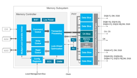
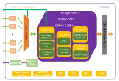
DDR5 Controller - Ensures high-speed, efficient operation and compatibility of memory controllers
- DDR5 Verification IP supports data rates up to 8400 MT/s, ensuring high-performance memory controllers meet the latest standards for speed, capacity, and power efficiency. It is designed to validate advanced features such as error correction and power management.
- This tool is ideal for validating DDR5 controllers in applications ranging from high-performance computing to mobile devices, ensuring robust performance and seamless integration in various systems
-
-
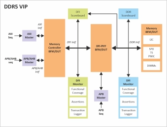
Simulation VIP for DDR5
- Speeds
- 3200, 3600, 4000, 4400, 4800, 5200, 5600, 6000, and 6400
- Density
- 8Gb, 16Gb, 24Gb, 32Gb, and 64Gb
-
DDR5 IP solution
- Compatible with DDR5 up to 4800Mbps
- AXI compliant multi-ports, and data width, FIFO depth, command queue depth configurable
- DFI5.0/4.0 compliant interface between controller and PHY
- Support ECC (error correcting code)
-
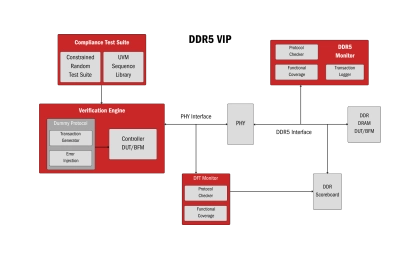
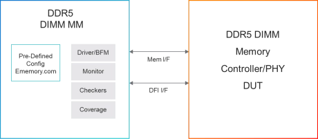
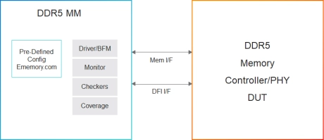
DDR5 RDIMM Verification IP
- The DDR5 RDIMM Verification IP provides an effective & efficient way to verify the components interfacing with DDR5 RDIMM interface of an ASIC/FPGA or SoC.
- The DDR5 RDIMM VIP is fully compliant with Standard DDR5 specification from JEDEC.
- This VIP is a light weight with an easy plug-and-play interface so that there is no hit on the design time and the simulation time.

-
DDR5 LRRDIMM Verification IP
- Compliant to JEDEC DDR5 SDRAM Specification, Data Buffer & RCD Specification.
- Supports connection to any DDR5 Memory Controller IP communicating with a JEDEC compliant DDR5 Memory Model.
- Supports configurable SDRAM addressing of different sizes (x4, x8 and x16).
- Available in all memory sizes up to 64 Gb.
- Supports for all speed-grades/speed-bins.
-
DDR5 DFI Synthesizable Transactor
- Compliant with DFI 5.0 Specification.
- DFI-DDR5 Applies to :
- DDR5 protocol standard JESD79-5 & JESD79-5 Rev1.40 (Draft) Specifications
- Supports all Interface Groups.