Clocking IP for SMIC
Welcome to the ultimate
Clocking IP
for
SMIC
hub! Explore our vast directory of
Clocking IP
for
SMIC
All offers in
Clocking IP
for
SMIC
Filter
Compare
110
Clocking IP
for
SMIC
from
13
vendors
(1
-
10)
-
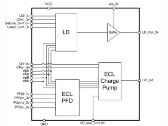
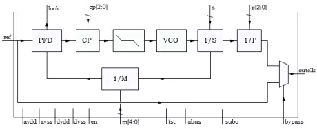
50MHz to 800MHz Integer-N RC Phase-Locked Loop on SMIC 55nm LL
- 055SMIC_PLL_01 forms clock output signal with frequency from 50 to 800MHz.
- It consists of the ring VCO with frequency from 400 to 800MHz, a programmable feedback divider, a low noise digital phase noise detector (PFD), a precision charge pump (CP) with internal loop filter, lock detector (LD) and programmable clock divider to obtain a required output frequency.
- LO output signal is CMOS compatible.
-
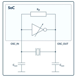
Crystal Oscillators
- The crystal oscillator macros are available in a wide range of industry-standard quartz crystals and MEMS resonators operating in the fundamental mode in the 32 kHz to 80 MHz range.
- These oscillators, which are both power and area efficient, have a programmable transconductance to allow users to find the optimal balance between jitter and power consumption.
-
Free running oscillators
- Compact and low power
- No external components
- Baseline CMOS logic process masks only
- Excellent frequency precision over PVT after trimming
-
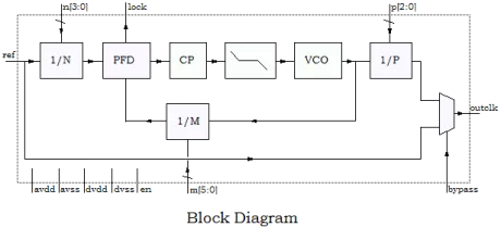
General Purpose PLL for TSMC 152nm
- Wide range M integer divider. (See ot3122 for M, N, and P dividers)
- 40MHz – 800MHz output frequency range.
- Comparable frequency range 8MHz – 32MHz.
- Optional prescaler.
- 19pS RMS cycle to cycle jitter at 800MHz.
- Lock-detect function.
- Bypass function.
- 20µS well defined fast startup behavior.
-
PLL for TSMC 130nm LP
- Wide range N, M, P integer dividers.
- 40MHz – 600MHz output frequency range.
- Comparable frequency range 8MHz – 50MHz.
- 18pS RMS cycle to cycle jitter at 400MHz.
- Lock-detect function.
- Bypass function.
- Well defined startup behavior.
- -40°C to 125°C temperature operation.
- Small cell area: 0.022mm2 in 0.13µ CMOS.
-
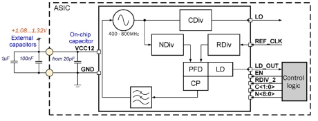
Phase-locked loop system 2.8 to 3.3 GHz
- SMIC CMOS 0.18 um
- Wide frequency range (2.8…3.3 GHz)
- Built-in switched capacitors sections for VCO frequency adjustment
- Low noise figure
-
7 to 150 MHz digitally controlled oscillator
- SMIC CMOS 180 nm
- Wide oscillation frequency adjustment range (7 MHz…150 MHz)
- No external components required
- Portable to other technologies (upon request)
-
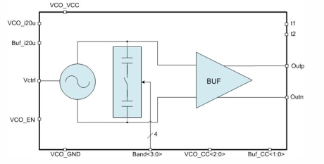
2.8 to 3.3 GHz Voltage controlled oscillator
- SMIC CMOS 0.18 um
- Wide frequency range (2.8…3.3 GHz)
- Wide range of control voltage (300…1500 mV)
- Built-in switched capacitor sections for VCO frequency adjustment
-
PLL system, 2.8 to 3.3 GHz
- SMIC CMOS 0.18 um technology
- Wide frequency range (2.8…3.3 GHz)
- Built-in switched capacitors sections for VCO frequency adjustment
- Low noise figure
-
24.84 MHz phase-frequency detector with charge pump
- SMIC CMOS 0.18 um
- Charge pump current control (40 uA, 60 uA, 80 uA, 100 uA)
- Wide range of charge pump output voltage (0.3 V…1.56 V)
- PFD polarity selection