The Memory Imperative for Next-Generation AI Accelerator SoCs
The tremendous growth in large language model (LLM) size corresponds with an equally dramatic rise in agentic AI applications, which are being adopted rapidly across both enterprise and consumer markets. To accommodate this demand, hyperscale providers are deploying next-generation data centers at an unprecedented rate and scale. Each of these data centers hosts millions of AI accelerators to run agentic AI workloads. One notable example is Meta’s Hyperion data center, which is projected to consume up to 5GW of compute power in a footprint that would cover a significant portion of Manhattan.
AI accelerators are key components of the AI data center tasked with speeding up the complex mathematical calculations required for AI and machine learning (ML). As the demand for AI continues to skyrocket, it’s crucial that SoCs provide the necessary “brain power” for these AI accelerators to keep pace. In this dynamic environment, SoC architects must carefully balance multiple factors to optimize their next-generation designs. When faced with the task of defining SoCs for tomorrow’s AI accelerators, four key criteria warrant close consideration: performance, power efficiency, SoC layout optimization, and futureproofing.
Performance
Next-generation LLMs, which can reach up to 100-trillion-parameter scale and beyond, demand exceptional computational throughput. While compute subsystems are advancing at an estimated 20X every two years, memory subsystems are improving only 2–3X over three years, creating what the industry now calls the memory wall.
In the face of this challenge, high-bandwidth memory (HBM) remains the preferred solution with its wide I/O architecture and superior performance. The latest HBM standard, HBM4, doubles the number of data lines from 1,024 to 2,048 compared to the previous generation (HBM3). This enables a significant increase in memory bandwidth (2X just due to doubling the data bits), unlocking higher overall AI accelerator performance.
Another key performance metric is memory data rate. The HBM4 standard increases the per-bit data rate to 8Gbps, from 6.4Gbps in HBM3. However, DRAM vendors are quickly moving beyond this speed due to the ever-increasing performance requirements of AI accelerators. To achieve these speeds, SoC developers require a memory subsystem, including a memory controller and physical layer (PHY), that can perform at or beyond the DRAM speed to ensure adequate system margin and high reliability. For example, in April 2025, Cadence announced an HBM4 PHY and controller that perform at 12.8Gbps, or 3.3TB/s of memory bandwidth, per HBM4 DRAM device. At this speed, AI hardware developers will have 4X the memory bandwidth available per DRAM when compared to the previous generation! The industry is not stopping, so expect to see even higher speeds to support AI’s insatiable demand for memory bandwidth.
Power Efficiency
Electricity is a major operational cost for modern data centers. In addition to powering SoCs and racks, data center operators must account for substantial cooling infrastructure and the power required to run it. With future AI/ML workloads measured in terabytes/s, power-efficient data transfers are even more critical for managing cost and improving sustainability.
For memory subsystems, efficient data movement between the SoC and HBM plays a critical role in overall power consumption. Measured in picojoules per bit (pJ/bit), lower energy-per-bit transfer directly enables higher energy efficiency, reduced cooling requirements, and lower total cost of ownership (TCO). By minimizing pJ/bit at the HBM PHY, systems achieve meaningful power savings that support sustainability goals while improving operational economics.
SoC Layout Optimization
In modern AI-centric SoCs, the core area is the most valuable real estate. Achieving higher AI performance depends on maximizing the silicon allocated to core logic—where the AI compute subsystem resides—while minimizing the footprint of the memory subsystem, which must still deliver massive bandwidth. As a result, both the SoC core area and shoreline must be extremely efficient to achieve peak performance.
Today’s AI SoCs are frequently designed at or near the reticle limit. At this scale, die edges must fit as many HBM4 PHYs as possible to maximize memory bandwidth per SoC while minimizing impact on compute core die area. Figure 1 illustrates an AI SoC layout with the HBM4 physical layers utilizing the area on the east and west sides of the die, with the compute core in the center. The long and narrow PHY layout efficiently uses the die edges with minimal waste between PHYs, while preserving valuable core logic space. In this example, the SoC will have 20TB/s memory bandwidth available with a 12.8Gbps memory subsystem.
Optimizing HBM4 PHY dimensions is more than just a packaging concern. It is a fundamental design decision that directly impacts AI performance, scalability, and silicon efficiency.
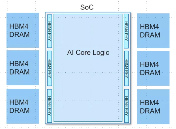
Figure 1: Example SoC layout optimized for maximum bandwidth
Futureproofing
With SoC design and fabrication cycles spanning 12 to 24 months, products designed today must anticipate the availability of faster DRAM devices at the time of system deployment. This means that SoC designs should incorporate HBM4 PHY and controller technology capable of supporting the highest speed grades today while being able to scale seamlessly as future DRAM generations become available.
At Cadence, we specialize in tackling these detailed design challenges. We are ready to provide the necessary technical information and support to quickly start your next-generation memory subsystem design. To see our industry-leading HBM IP in action, visit us at Booth 300 at the 2026 Chiplet Summit, where we’ll be demonstrating our 3nm HBM3E PHY operating at 14.4Gbps.
Learn more about Cadence’s HBM4 PHY and Controller IP.
Related Semiconductor IP
- HBM4E PHY and controller
- HBM 4 Verification IP
- Verification IP for HBM
- Simulation VIP for HBM
- HBM Synthesizable Transactor
Related Blogs
- The Silent Guardian of AI Compute - PUFrt Unifies Hardware Security and Memory Repair to Build the Trust Foundation for AI Factories
- The Architectural Evolution of 16GHz PLLs for Next-Gen AI and SerDes SoCs
- The Architectural Evolution of 16GHz PLLs for Next-Gen AI and SerDes SoCs
- HBM4 Boosts Memory Performance for AI Training
Latest Blogs
- A Bench-to-In-Field Telemetry Platform for Datacenter Power Management
- IDS-Verify™: From Specification to Sign-Off – Automated CSR, Hardware Software Interface and CPU-Peripheral Interface Verification
- RISC-V and GPU Synergy in Practice: A Path Towards High-Performance SoCs from SpacemiT K3
- EDA AI Agents: Intelligent Automation in Semiconductor & PCB Design
- Why Security Can't Exist Without Trust