HBM4 Boosts Memory Performance for AI Training
The recent HBM4 specification announced by JEDEC is great news for developers of AI training hardware. HBM4 is the latest specification in the rapidly evolving High Bandwidth Memory (HBM) DRAM standard, providing 2TB/s of memory performance and higher density up to 64GB (32Gb 16-high), according to JEDEC. "The advancements introduced by HBM4 are vital for applications that require efficient handling of large datasets and complex calculations, including generative artificial intelligence (AI), high-performance computing, high-end graphics cards, and servers," said the JEDEC release.
Large language model (LLM) data sets are growing exponentially, and current CPU and GPU performance is often limited by the available memory bandwidth. Because of this "memory wall," HBM has become the memory of choice for generative AI training due to its superior bandwidth, capacity, and memory efficiency.
HBM4 builds on HBM3 (and HBM2E) standards, which are widely deployed in AI training hardware in the data center. HBM4 offers a 2X improvement in memory bandwidth over HBM3. The bandwidth improvement is achieved by increasing both the frequency to 8Gb/s (6.4Gb/s for HBM3) and doubling the number of data bits to 2048 bits (from 1024 bits in HBM3). The total bandwidth is now boosted to 2TB/s, which is needed for AI training hardware.
In addition to bandwidth, the HBM4 standard addresses key issues in the data center, including the growing size of LLM data sets, reliability, and memory efficiency. To support these growing data sets, HBM4 provides additional capacity supporting up to 16-high DRAM stack configurations with per-stack die densities of 24Gb or 32Gb. The maximum combination of die density (32Gb) and stacks (16-high) provided a total cube density of 16x32Gb or 64GB. To address reliability, availability, and serviceability (RAS), HBM4 incorporates direct refresh management (DRFM) for improved row-hammer mitigation. And finally, for better memory efficiency, HBM4 increased the number of channels supported to 32, with two pseudo-channels per channel, providing more flexibility for different data types.
In conjunction with the JEDEC announcement, Cadence is releasing its first HBM4 memory PHY and controller IP product with a best-in-class data rate of 12.8Gbps. At 12.8Gbps, this new product exceeds the maximum DRAM device speed, giving designers ample system margin and future-proofing their designs for potential speed increases.
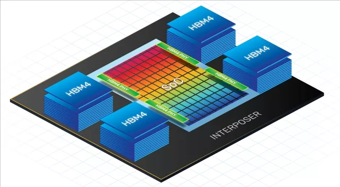
The bandwidth advantage of HBM4 also comes with the challenge of routing 2048 data bits (plus control bits) to the processor. As with HBM3, routing these signals requires some type of interposer technology. Silicon interposers are the most common and will require additional signal and ground layers to accommodate the increased number of bits. To take full advantage of these high data rates and wider data buses, the interposer design is critical to system performance. The correct placement of signals and grounds is necessary for strong signal integrity and power integrity (SI/PI) to mitigate effects like signal crosstalk. To speed up the system design, Cadence provides an interposer and package reference design. In addition, Cadence system and SI engineers work closely with customers to guide them through the design, ensuring the highest performance and the best signal margin.
Cadence has been the HBM performance leader in shipping HBM3 products since 2022, with our latest HBM3 product at speeds of 10.4Gb/s. Cadence is proud to continue this leadership with the latest HBM4 PHY and Controller at 12.8Gb/s.
Learn more about Cadence's Memory IP.
Related Semiconductor IP
Related Blogs
- HBM4 Elevates AI Training Performance To New Heights
- Link Training: Establishing Link Communication Between DisplayPort Source and Sink Devices
- HBM2E targets AI/ML training
- Rambus HBM3 Controller IP Gives AI Training a New Boost
Latest Blogs
- IDS-Verify™: From Specification to Sign-Off – Automated CSR, Hardware Software Interface and CPU-Peripheral Interface Verification
- RISC-V and GPU Synergy in Practice: A Path Towards High-Performance SoCs from SpacemiT K3
- EDA AI Agents: Intelligent Automation in Semiconductor & PCB Design
- Why Security Can't Exist Without Trust
- Universal Browser Support for JPEG XL: Is Your Hardware Ready for the New Standard?