Synopsys Interconnect IPs Enabling Scalable Compute Clusters
Recent advancements in machine learning have resulted in improvements in artificial intelligence (AI), including image recognition, autonomous driving, and generative AI. These advances are primarily due to the ability to train large models on increasingly complex datasets, enabling better learning and generalization as well as the creation of larger models. As datasets and model sizes grow, there is a requirement for more powerful and optimized computing clusters to support the next generation of AI.
With more than 25 years of experience in delivering field-proven silicon IP solutions, we are thrilled to partner with NVIDIA and the NVIDIA NVLink ecosystem to enable and accelerate the creation of custom AI silicon. This strategic collaboration will leverage Synopsys' expertise in silicon IPs to assist in the development of bespoke AI silicon, forming the foundation for advanced compute clusters aimed at delivering the next generation of transformative AI experiences.
Compute challenges with larger datasets and increasingly large AI models
Training trillion-parameter-plus models on large datasets necessitates substantial computational resources, including specialized accelerators such as Graphics Processing Units (GPUs) and Tensor Processing Units (TPUs). AI computing clusters incorporate three essential functions:
- Compute — implemented using processors and dedicated accelerators.
- Memory — implemented as High Bandwidth Memory (HBM) or Double Data Rate (DDR) with virtual memory across the cluster for memory semantics.
- Storage — implemented as Solid State Drives (SSDs) that efficiently transfer data from storage to processors and accelerators via Peripheral Component Interconnect Express (PCIe)-based Network Interface Cards (NICs).
Retimers and switches constitute the fabric that connects accelerators and processors. To enhance the computational capabilities of the cluster, it is necessary to increase capacity and bandwidth across all functions and interconnects.
Developing increasingly sophisticated, multi-trillion-parameter models requires the entire cluster to be connected over a scale-up and scale-out network so it can function as a unified computer.
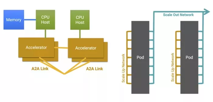
Figure 1: A representative compute cluster with scale-up and scale-out network.
Standards-based IPs for truly interoperable compute clusters
The successful deployment of next-generation computing clusters relies on silicon-verified interconnects that utilize advanced process node technology and guarantee interoperability. Standardized interconnects enable an interoperable, multi-vendor implementation of a cluster.
PCIe is an established standard for processor-to-accelerator interfaces, ensuring interoperability among processors, NICs, retimers, and switches. Since 1992, the PCI-SIG has been defining Peripheral Component Interconnect (PCI) solutions, with PCIe now in its seventh generation. The extensive history and widespread deployment of PCIe ensure that IP solutions benefit from the silicon learning of previous generations. Furthermore, the entire ecosystem developing processors, retimers, switches, NICs, and SSDs possesses significant deployment experience with PCIe technology. Our complete IP solution for PCIe 7.0 is built upon our experience with more than 3,000 PCIe designs, launched in June 2024 with endorsements from ecosystem partners such as Intel, Rivos, Xconn, Microchip, Enfabrica, and Kandou.
When deploying trained models in the cloud, hyperscalers aim to continue utilizing their software on custom processors that interface with various types of accelerators. For NVIDIA AI factories, NVLink Fusion provides another method for connecting processors to GPUs.
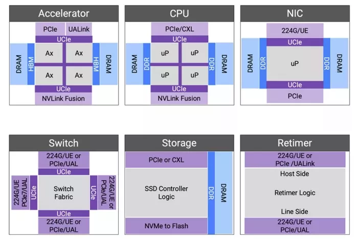
Figure 2: Components and interconnects of a next-generation compute cluster.
Accelerators can be connected in various configurations, affecting the efficiency of compute clusters. Scale-up requires memory semantics for a virtual memory pool across the cluster, while scale-out involves connecting tens-of-thousands to hundreds-of-thousands of GPUs with layers of switching and congestion management. Unlike scale-up, scale-out is more latency-tolerant and designed for bandwidth oversubscription to suit AI model data parallelism. In December 2024, we launched our Ultra Accelerator Link (UALink) and Ultra Ethernet solution to connect accelerators efficiently. The solution, which was publicly supported with quotes from AMD, Juniper and Tenstorrent, is based on silicon-proven 224G PHY and more than 2,000 Ethernet designs.
Trillion-parameter models demand extensive memory storage and high data rates for low latency access, necessitating increased memory bandwidth and total capacity. HBM provides both substantial capacity and high bandwidth. Our HBM4 IP represents the sixth generation of HBM technology, offering pin bandwidths up to 12 Gbps, which results in an overall interface bandwidth exceeding 3 TBps.
Co-packaged multi-die aggregation not only enhances compute throughput by overcoming the limitations of advanced fabrication processes but also facilitates the integration of optical interconnects through emerging Co-Packaged Optical (CPO) technologies. Since 2022, we have been developing linear electro-optical (EO) interfaces to create energy-efficient EO links. The Universal Chiplet Interconnect Express (UCIe) standard has provided a well-defined path for multi-vendor interoperability. In collaboration with Intel in 2023, we successfully demonstrated the first UCIe-connected, chiplet-based test chip.
Multi-die integration poses challenges for heat dissipation, potentially impacting temperature-sensitive photonic components or causing thermal runaway. Our comprehensive multi-die solution, including Die-to-Die IP, HBM IP, and 3DIC Compiler for system-in-package integration, provides a reliable and robust multi-die implementation.
Adopting well-established and extensively validated IP solutions across critical interconnects – from processor-accelerator interfaces to advanced multi-die architectures and HBM – mitigates the risks associated with custom design and integration. Pre-verified IPs streamline the design and verification process, accelerate timelines, and ultimately pave the way for successful first-pass silicon, enabling the rapid deployment of innovative and interoperable compute clusters.
Related Semiconductor IP
- PCIe 7.0 PHY, TSMC N3P x4, North/South (vertical) poly orientation
- 1.6T/3.2T Multi-Channel MACsec Engine with TDM Interface (MACsec-IP-364)
- NFC wireless interface supporting ISO14443 A and B with EEPROM on SMIC 180nm
- NFC wireless interface supporting ISO14443 A and B on SMIC 180nm
- PSI5 IP Core Controller for Peripheral Sensor Interface 5 Communication
Related Blogs
- How AI Is Enabling Digital Design Retargeting to Maximize Productivity
- PCIe 6.x and 112 Gbps Ethernet: Synopsys and TeraSignal Achieve Optical Interconnect Breakthroughs
- Verification of UALink (UAL) and Ultra Ethernet (UEC) Protocols for Scalable HPC/AI Networks using Synopsys VIP
- Adapting Foundation IP to Exceed 2 nm Power Efficiency in Next-Gen Hyperscale Compute Engines
Latest Blogs
- From driveway to checkout: seamless indoor navigation powered by UWB
- Serial Wire Debug (SWD) Protocol: Efficient Debug Interface for Arm-Based System
- ChiPy®: Bridge Neural Networks and C++ on Silicon — Full Inference Pipelines with Zero CPU Round-Trips
- Securing RISC-V Third-Party IP: Enabling Comprehensive CWE-Based Assurance Across the Design Supply Chain
- Power, Not Area: Why Edge GPU Design Is Entering a New Era