EOS protection characterization using Long-Pulse TLP

EOS, or Electrical Overstress, is a significant factor in IC reliability. Sometimes, IC interfaces and/or power pads are subjected to voltage/current levels beyond the absolute maximum rating. Sources claim that more than 40% of the field failures in electronic products are related to EOS.
Unlike Electrostatic Discharge (ESD), which is a short and sudden event, EOS arises from sustained or repetitive electrical stress. The duration of this type of stress is also longer in nature. A different type of characterization is needed to account for this difference in stress type. At Sofics we use long pulse TLP (LP-TLP) measurement to account for this difference. This extends the normal TLP pulse from the order of 100ns to a TLP pulse width of 1–2 µs.
Protection strategies
There are three approaches to design for EOS requirements:
- Increasing the voltage tolerance: This approach involves changing the I/O circuit and ESD protection clamps to increase the voltage tolerance of input/output drivers. This can be achieved by connecting multiple devices in series, using transistors with intrinsic higher voltage tolerance, or relying on a foundry process that offers high voltage options like NLDMOS transistors.
- Secondary protection approach: In this approach, IC designers keep the I/O circuits the same while changing only the ESD protection clamps to handle IEC 61000-4-5 requirements. The protection consists of three elements: a primary ESD protection with high voltage tolerance, isolation resistance, and a secondary ESD protection close to the I/O transistors.
- Relying on resistance in the test system: This approach involves using the standard interface circuits and ESD devices for each of the interfaces but relying on resistance in the test system to handle IEC 61000-4-5 requirements. IC designers use this resistance in a similar way as the secondary protection described in Approach 2, applying higher stress levels through the output resistance.
A detailed explanation of these 3 approaches can be found in this article here 3 approaches to handle EOS ‘requirements’.
When evaluating these protection strategies in practice, it becomes important to confirm that the intended current paths behave as expected under EOS stress. However from a design perspective, it is worth noting that if the protection clamp is not drawing EOS current, it is not necessary to characterize it. An example of such a case is shown in the fig. 1 bellow. In such cases the secondary clamp does not contribute to the system’s EOS behavior and the focus should instead be placed on the components that actually conduct the current.
This approach ensures that characterization efforts remain efficient and technically meaningful, emphasizing the true current-carrying elements that define EOS robustness.
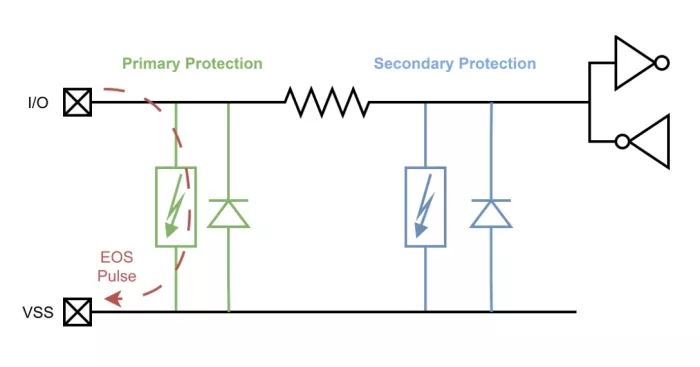
Figure 1. Shows an example of an EOS pulse where the pulse is only seen by the primary protection.
IEC 61000-4-5
This standard is already discussed in another article 3 approaches to handle EOS ‘requirements’ in the section “Case study: IEC 61000-4-5 requirement”.
There is an important note to make about this standard and the LP-TLP. In the IEC 61000-4-5 we are talking about system-level verification. The voltage levels are described in the table 1 and current levels ranging from 250A – 2000A, which correspond to voltage levels that are not relevant for single silicon devices. When comparing the two measurement setups, we have to be conscious about the difference in levels.
| Level | Open-circuit test voltage kV | Current seen by DUTA |
|---|---|---|
| 1 | 0.5 | 250 |
| 2 | 1.0 | 500 |
| 3 | 2.0 | 1000 |
| 4 | 4.0 | 2000 |
| X | Special | Special |
Note: X can be any level, above, bellow or in between the other levels. This level can be specified in product standard.
Table 1. Shows the IEC-6100-4-5 standard for different levels of the open-circuit test voltage and current seen by the device under test (DUT).
Long pulse TLP
The Long Pulse Transmission Line Pulse (LP-TLP) is a variation of the existing measurement setup Transmission Line Pulse (TLP) used in the industry today to characterize ICs and ESD protection devices. For reference, see the article Transmission Line Pulse (TLP) test system. With this new type we extend the pulse width from the standard 100ns to around 1–2µs. The inherent rise time of the LP-TLP system will also be longer compared to standard TLP (typically larger than 10ns). This is due to the rise time of the solid-state pulser combined with the parasitic inductance and capacitance introduced by the connectors.
The measurement setup is shown in fig. 2, where we have 50 Ohm terminations and switching between a high-voltage pulser and a leakage measurement of the DUT to monitor failure.
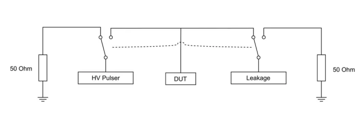
Figure 2. Shows the set-up for LP-TLP measurements
From this, we can summarize the main differences between LP-TLP and IEC 61000-4-5 to be:
- Rise times
- EOS: 1.2 µs – 8 µs
- LP-TLP: larger than 10 ns
- Peak current duration
- Voltage and current drawn with the pulse
- System-level vs. Device-level
In the previous section, we linked EOS voltage and EOS current using the IEC 61000-4-5 standard. In this section, we are not directly comparing the EOS voltage to LP-TLP voltage levels, but rather looking at the current that is generated in the device when exposed to EOS-type stress. The goal is to understand how the current delivered by the LP-TLP pulse corresponds to the current that would be produced under actual EOS stress conditions.
The characteristics of the two pulses are also quite different. LP-TLP is a square pulse and has a much faster rise time than the EOS pulse. With this estimation it can be seen as somewhat overdesigned for the EOS stress it was made to emulate. In most cases, this is not an issue, although it becomes more relevant when looking at low-capacitance devices. Since this is a device-level measurement compared to the system-level nature of IEC testing, one could argue about how much of the applied pulse the device itself actually experiences during EOS stress.
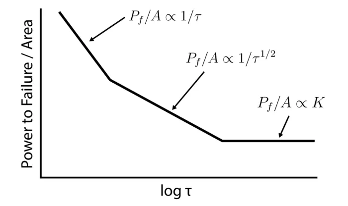
Figure 3. Voldman, S.H.. (1999). The State of the Art of Electrostatic Discharge Protection: Physics, Technology, Circuits, Design, Simulation, and Scaling. Solid-State Circuits, IEEE Journal of. 34. 1272 – 1282. 10.1109/4.782088.
Failure of the device depending on area and pulse width has been discussed in multiple articles of IC device characterization using different pulse types. In the fig. 3 we have the Wunsch-Bell curve, which describes the power to failure over area vs. log pulse width. In 3 distinct phases: phase 1 , phase 2 and phase 3 . With the data and curve we can look at the design, scaling and predictions of devices for the stress cases we are investigation.
Example of 1.8V Devices in 22nm process
Multiple devices were measured on 22nm process with the LP-TLP set-up. The pulse width was varied between 0.5μs to 2μs with an increment of 0.5µs. These devices were also measured on VF-TLP 10ns and TLP 100ns, to compare performance between the different measurement methods.
Further investigation was also conducted with pulse widths of 0.2μs, 0.3μs and 04.μs on some devices like the one shown in fig. 4. of 1.8V devices. From this we see that the current tapers down drastically when pulse width increases and is approaching a constant value for the failure current like in the Wunsch-Bell curve in fig. 3. Applying this theory to our data we observe that the RC triggered device is in phase 1 with the pulse width less than 0.25μs, 2nd phase 0.25μs to 1.5μs and phase 3 after this. It is similar for the diode triggered SCR, but here we would argue that there is no phase 1 only 2 and 3. With this there is no need to measure for longer pulse widths as we know from the Wunsch-Bell that this is a constant value. The second observation is the different behavior for different ESD clamp types. We saw that on average the decreasing factor in It2 for RC triggered devices is a lot larger then that of other trigger methods.
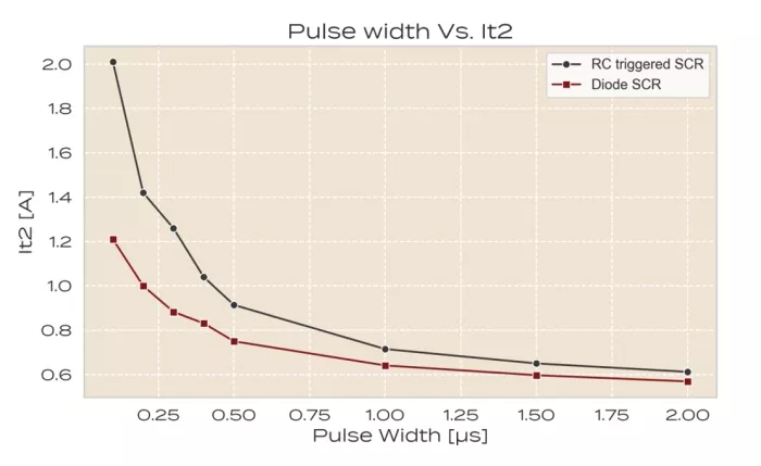
Figure 4. Shows a line plot of pulse width in μs and It2 in amps of 1.8V devices.
Its worth mentioning that both devices include MOS elements, where they differ is triggering. With RC device we refer to a timing pulse generated by a resistor and capacitor that is used as a trigger. The RC devices rely on the RC trigger of the MOS device, to trigger the SCR, where as the Diode-SCR devices use diode(s) to trigger.
During this investigation we measured multiple different structures to characterize their behavior. We tested multiple of Sofics proprietary solutions to better understand their behavior to learn under which conditions the different devices are most suitable.
Conclusion
Using LP-TLP measurements we can better understand how protection devices respond to longer-duration EOS stress compared to standard testing like TLP or VF-TLP. With this method we gain valuable insight into the current handling capability of the EOS clamp under realistic conditions. Bridging the gap between device-level and system-level testing defined by standards such as IEC 61000-4-5.
This approach allows designers to evaluate how the current scales with pulse duration and to identify trigger mechanisms, which could be sensitive to long-pulse stress. Such methods are essential when optimizing protection design for PPA&R Power-Performance-Area & Robustness.
With well established and evolving methods like LP-TLP, IC designers can build protection strategies that meet future requirements, while maintaining high reliability and performance across technology generations.
Related Semiconductor IP
Related Blogs
- Tips on Using e Macros to Raise Abstraction and Facilitate Reuse
- An inconvenient truth about using DDR3 SDRAM for embedded designs
- Some critical considerations for SoC and Silicon Realization teams thinking about using ARM Cortex-A7 or ARM Cortex-A8 processor cores
- Using Physical USB Devices with the Xilinx Zynq-7000 Virtual Platform
Latest Blogs
- The Silent Guardian of AI Compute - PUFrt Unifies Hardware Security and Memory Repair to Build the Trust Foundation for AI Factories
- Heterogeneous NPU Data Movement Tax: Intel's Own Slides Tell the Story
- PQMicroLib-Core now supports PSA Certified Crypto API
- Imagination Demonstrates DirectX Gaming on D-Series GPUs
- Embedded Security explained: Post-Quantum Cryptography (PQC) for embedded Systems