PCIe Low-Power Validation Challenges and Potential Solutions (PIPE/L1 Substates)
As chip complexities increase and the industry evolved to more battery-powered devices, power aware/consumption research becomes an integral part of design in the industries. Low power is crucial in ASIC applications to ensure longevity, durability, and reliability. PCI-SIG has focused on reducing power consumption while the PCIe interface is active to enable better platform power management (PM). In the blog below, we will focus on low-power substate verification challenges and solutions using verification IP (VIP).
Background
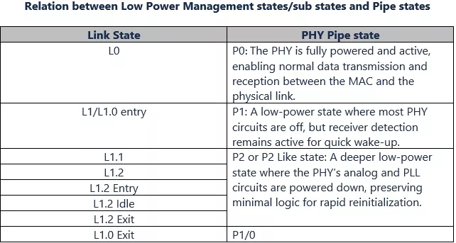
PCIe protocol defines the following link states:
- L0 – The fully active link state where normal data transmission and reception occur between endpoints
- L0s - A brief idle power-saving state where the transmitter is idle, but the receiver stays active for rapid return to L0. Not supported in Gen6 and above. Replaced by L0p
- L1 – A link power-saving state was signaling stops and most PHY circuits are off, but the link can quickly resume L0 when needed
- L1.0 - A low-power sub state where both ends stop data transmission, placing transmitters in electrical idle while maintaining receiver detection for quick wake-up to L0
- L1.1 - A deeper low-power sub state than L1.0 where most analog circuits are powered off, retaining minimal logic for faster recovery than L1.2
- L1.2 - The deepest L1 substate where both transmitter and receiver analog circuits are completely powered down, enabling maximum power savings with longer wake-up time
- L2 – A deep power-down state where the link is inactive and most circuitry is off, awaiting reactivation through reset or wake events
PCIe PHY defines the PIPE states that represent power and operational modes that control link’s electrical activity ranging from P0 (active data transmission) to progressively lower-power idle states like P1, P2/P2L, and P3, which shut down portions of the PHY to save power.
Verification challenges with current low-power states
Profound validation of power management states includes low-power substates across PHY, Pipe Macro, and MAC configurations using customer desired out-of-spec power-down values enabling commissioned power savings as per DUT implementation. Verification engineers often need timing hooks to control PIPE signals to configure time spent in low-power states. Events such as surprise reset, Hot Reset, PME_TurnOff, or CLKREQ# can interrupt power states. Graceful exit from power down states using reference clock to completely operational state validation is critical in ensuring resumption of traffic.
Potential solution to these challenges
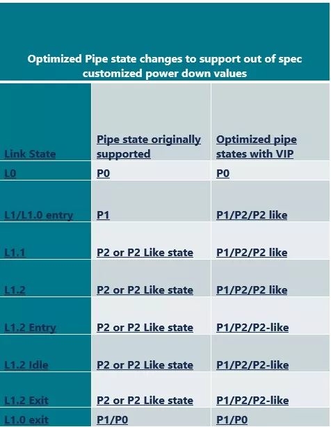
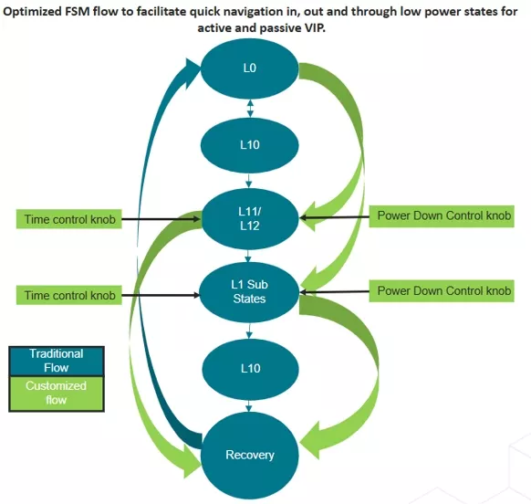
Drive power-down values / pipe signals as per customized DUT behavior (supporting optimized pipe states with link states as shown in table below). Validate instant power savings for DUT by supporting transitions to enter and exit low-power states not strictly adhering to traditional flow (as demonstrated in optimized FSM flow diagram). Using a monitor (passive agent) independent of active VIP for verifying out-of-spec power down objectives, designing customized wake-up scenarios from low-power states and validating DUT for extended as well as minute time spent in low-power states. The VIP provides a configurable delay parameter for each low-power sub-state, allowing users to simulate realistic power-down timing and verify handshake dependencies during low power. VIP also supports mapping L1 substate to different combinations of RxEIDetectDisable and TxCommonModeDisable side band signals while the power-down value is kept to a specific value of P2/P2 like state.
Summary
Allowing users to configure any power-down value for any low-power substates (e.g., allowing P2/P2 like power-down values even when low-power substates not enabled), skipping different power-down values when entering or exiting low-power substates translating to swifter transitions in and out of low-power states, and providing configurability and controllability knobs to adjust time and power-down values in low power substates, enables customers to validate their DUT comprehensively for low-power substates using verification IP,
Cadence PCIe VIP offers all the above solutions with a rich test suite, allowing customers to navigate the challenges of low power in the early stages (simulation) of chip validation.
More information
For more info on how Cadence PCIe Verification IP and Triple Check VIP help users confidently verify low-power applications, see our webpages on VIP for PCI Express, VIP for Compute Express Link, and TripleCheck for PCI Express
See the PCI-SIG website for more details on PCIe in general and the different PCI standards.
Related Semiconductor IP
- Configurable PCI Express 4.0 Link Controller
- PCI Express PHY
- Multi-Channel Flex DMA IP Core for PCI Express
- PCIe - PCI Express Controller
- PCI Express PIPE PHY Transceiver
Related Blogs
- Randomization considerations for PCIe Integrity and Data Encryption Verification Challenges
- Embarrassingly Parallel Problems: Definitions, Challenges and Solutions
- Cadence PCIe Solutions: Configurable, Compliant, and Low Power
- How to Overcome NoC Validation Multiple Challenges?
Latest Blogs
- Area, Pipelining, Integration: A Comparison of SHA-2 and SHA-3 for embedded Systems.
- Why Your Next Smartphone Needs Micro-Cooling
- Teaching AI Agents to Speak Hardware
- SOCAMM: Modernizing Data Center Memory with LPDDR6/5X
- Bridging the Gap: Why eFPGA Integration is a Managed Reality, Not a Schedule Risk