Breaking the Bandwidth Barrier: Enabling Celestial AI’s Photonic Fabric™ with Custom ESD IP on TSMC’s 5nm Platform

Prepared by Wouter Faelens, Emil Hågan, Bart Keppens with the help of Celestial.AI contacts. Presented live at the 2025 TSMC OIP Forums in Japan, Taiwan and Europe.
The Problem: AI’s Exponential Appetite for Bandwidth
 The semiconductor industry is no stranger to scaling challenges. Since the seventies the industry has been following Moore’s law with doubling of the compute performance every 2 years. Despite frequent call for “the end of Moore’s law” the industry has been able to continue this trend.
Yet in recent years, the rise of generative AI and massive-scale models has exposed a new fundamental bottleneck: memory bandwidth.
While compute performance (FLOPS) continues to scale, driven by GPUs, TPUs, and custom accelerators, the ability to move data between compute and memory is not keeping up.

Figure 1: [Dark blue] Dramatic increase of the number of parameters in the AI models over the years. [Light Blue] Increase in the memory capacity of the compute processors. Mind that the vertical axis is a log-scale. Even the memory capacity is increasing exponentially. from: https://medium.com/riselab/ai-and-memory-wall-2cb4265cb0b8
In the graph (based on work by RiseLab and Meta) in Figure 1, the time (horizontal axis) is split in two era’s. The vertical axis is a logarithmic scale for model size (number of parameters) and memory capacity. Till about 2019 we lived in the compute limited era. The increase in AI capabilities was limited by increases in compute capabilities. From 2019 on the popular AI models have more parameters than the memory capacity of the most performant AI systems. This brings us to the memory and bandwidth era.
The chart shows the widening gap between compute and memory bandwidth. This “Memory Wall” now limits AI scalability more than any other factor. As model sizes explode beyond 1Tera parameters, a radical shift is needed: not just faster chips, but faster interconnects.
Enter Optical Interconnects: Photons, Not Electrons
The obvious answer is optical connections. Photons move faster, farther, and more efficiently than electrons over copper traces. Many of the recent AI designs incorporate photonics to speed up data movement. Earlier in 2025, Nvidia presented their co-packaged photonics solutions and roadmap for the next 10 years. They reached nearly 18 Tbps off-package bandwidth and are scaling it to more than 400 Tbps in the next 10 years. The vertical axis in the figure 2. is again a logarithmic scale. TSMC has added their ‘COUPE’ platform to help chip developers to incorporate optical links.
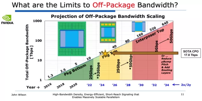
Figure 2: increase in total off-package bandwidth for Nvidia chips. In 2025 their Co-packaged photonics reached nearly 18 Tbps. They project to reach close to 400 Tbps by 2034.
But traditional optical solutions bring their own challenges:
- They require large “beachfront” areas at the edge of the die
- Depend on digital signal processing (DSP) and re-timer circuits, adding latency and power
- Struggle to support dense packaging or chiplets
In other words, they work, but they don’t scale with the silicon.
The Photonic Fabric™: Celestial AI’s Game-Changer
That’s where Celestial AI comes in. Their Photonic Fabric™ is a breakthrough full-stack interconnect platform designed from the ground up for AI scale. What makes it different?
- No DSP required: linear drive optics with high signal to noise ratio (SNR) and low bit rate error (BER)
- Thermally stable optical modulators that can operate directly under hot compute ASICs
- Data delivered anywhere on-die, not just at the edge, eliminating round-trip latency
- Integrated within TSMC 4nm and 5nm processes for the electric IC (EIC) on top of the photonic interposer (the PIC)
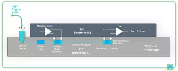
Figure 3: Celestial.AI’s Photonic Fabric: The EIC, on e.g. 4nm or 5nm FinFET technology is mounted on top of the PIC photonic interposer.
Besides innovations in the EIC one of the key aspects of the Photonic Fabric is in the photonic interposer (PIC). They developed another modulator. MZI modulators can be thermally stable enough to be placed under a ‘hot’ chip but they are typically rather large and consume a lot of power. Ring modulators on the other hand consume little power, are very small but the operation is not stable across different temperatures and only work for a narrow optical bandwidth. The EAM structure in the Celestial AI approach combines the best of the characteristics.
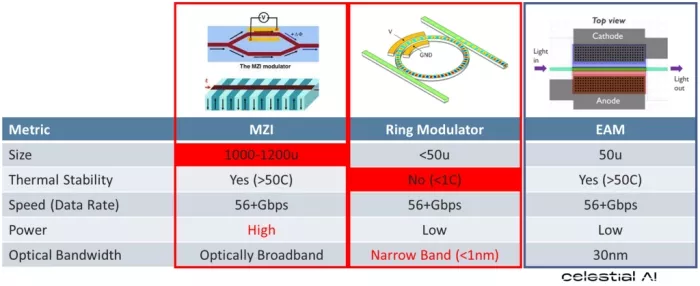
Figure 4: Different modulation techniques used in the PIC. Celestial.AI uses the EAM modulation because it is small, uses low amount of power and its operation is very stable across a broad temperature range. That enables its use below the ASIC.
This innovation enables; chiplet-to-chiplet, within-package, and package-to-package optical connections, all at bandwidths beyond 50 Gbps, with latencies measured in nanoseconds.
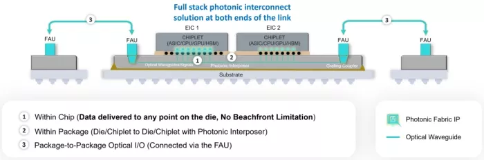
Figure 5: Photonic Fabric enables photonic communication within a single EIC chiplet, between chiplets on the same photonic interposer and to other devices across a fibre optic cable.
In fact, the Photonic Fabric platform has the potential to deliver 390 Tbps off-package bandwidth, more than 20x the current co-packaged optics state of the art.
Behind the scenes: ESD protection and the role of Sofics
While optical data movement sounds elegant, building it in silicon is anything but simple.
Celestial AI needed specialized ESD and I/O protection IP. Those solutions that don’t exist in foundry standard libraries. That’s where Sofics stepped in.
Why standard GPIO/ESD libraries won’t work:
- Optical transmitter and receiver TX/RX circuits use low voltage (~0.9–1.0V) and some also require higher voltages, beyond the 1.5V that is supported by the foundry.
- Need to maintain signal integrity at >50 Gbps
- Cannot tolerate high parasitic capacitance (>20fF)
- Interfaces use thin-oxide devices, which are ESD sensitive
- Require compact area for dense 2.5D and 3D packaging
What Sofics Delivered:
- Low-capacitance ESD IP (<14fF) optimized for 5nm
- 50V CDM robustness with <100nA leakage
- Footprint: just 10μm × 13μm
- Custom analog domain clamps for 1.8V and 3.3V with full 1kV HBM protection
These blocks were validated on TSMC 5nm MPW silicon, built on years of Sofics experience with over 40 datacenter and AI projects, including multiple photonics and timing chips.
Engineering Details: Capacitance vs ESD Robustness
Sofics’ IP pushes the boundaries of capacitance-to-robustness ratio. Our custom ESD cells achieve up to 80% lower parasitic capacitance than traditional solutions for the same level of ESD protection, a vital enabler for 50+ Gbps links.
We have delivered silicon-proven results across TSMC 28nm, 7nm, 5nm, and even exploratory nodes like N2. For chiplets, MEMS combos, and automotive-grade designs, we customize the right ESD-IP fit.
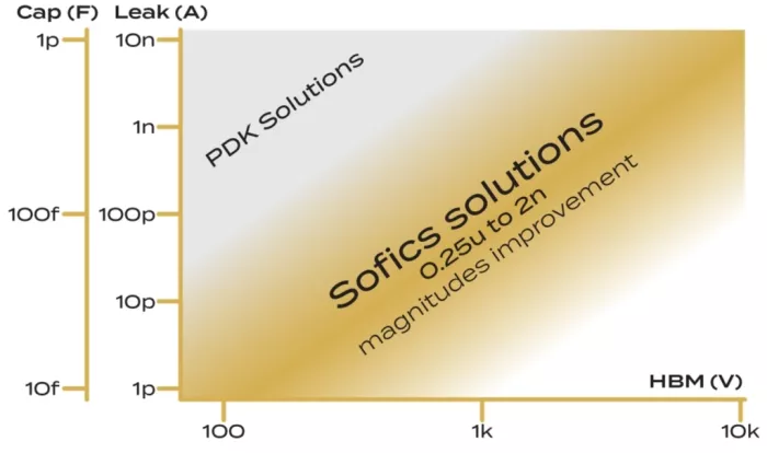
Figure 6: ESD protection solutions for different ESD robustness levels (horizontal axis using logarithmic scale) and parasitic capacitance and leakage (vertical axis using logarithmic scale). Sofics IP solutions validated on silicon and/or delivered to customers fall within the golden band, with both leakage and capacitance that is order(s) of magnitude lower than traditional or foundry provided ESD clamps.
Powered by the TSMC Ecosystem
None of this would have been possible without the support of TSMC and their Open Innovation Platform (OIP). The combination of TSMC’s advanced silicon nodes, MPW access, and IP Alliance programs enabled:
- First-pass silicon validation
- Seamless IP integration across photonics and electronics
- Ecosystem collaboration between ASIC, packaging, and IP providers
Final Takeaways
It is clear, when we want to scale AI workloads we need faster access to memory. Optical interconnects are being investigated by many as the key solution to enable that. The leaders in AI like Nvidia are employing that already in their most recent solutions with Co-packaged Photonics (CPO) solutions reaching 18 Tbps total off-package bandwidth in 2025 and scaling to 400 Tbps in 10 years. Unfortunately there are drawbacks to the CPO approach.
Celestial.AI developed a novel approach where the photonic elements can be below the main AI-compute ASIC which leads to unmatched performance potentially reaching 400 Tbps already in 2026. That is probably one of the reasons Marvell decided to acquire Celestial end of 2025.
For their 4nm/5nm EIC they required small area, low-capacitance ESD clamps that protect thin oxide transistors, a perfect challenge for the Sofics technology. Thanks to the collaboration with TSMC that IP was already proven on silicon a few years earlier.
Explore ESD IP:
- On-chip ESD/EOS/Latch up protection for advanced and low voltage processes
- On-chip ESD/EOS/Latch up/EMC protection for high voltage and BCD processes
- Robust circuit and interface solutions
Related Semiconductor IP
- On-chip ESD/EOS/Latch up protection for advanced and low voltage processes
- On-chip ESD/EOS/Latch up/EMC protection for high voltage and BCD processes
- Robust circuit and interface solutions
- Stand-Alone ESD Cell in GF 28nm
- Analog I/O Library with a custom 12V ESD Solution IN GF 55nm
Related Blogs
- How Synopsys IP and TSMC's N12e Process are Driving AIoT
- Imagination DXTP GPU IP: Accelerating Games and AI Apps All. Day. Long.
- Cadence Silicon Success of UCIe IP on Samsung Foundry’s 5nm Automotive Process
- Skymizer Reduces Verification Cycles for AI Accelerator IP Development by 33% with Synopsys HAPS Prototyping
Latest Blogs
- Ensuring reliability in Advanced IC design
- A Closer Look at proteanTecs Health and Performance Management Solutions Portfolio
- Enabling Memory Choice for Modern AI Systems: Tenstorrent and Rambus Deliver Flexible, Power-Efficient Solutions
- Verification Sanity in Chiplets & Edge AI: Avoid the “Second Design” Trap
- Embedded Security explained: Cryptographic Hash Functions