Cadence Silicon Success of UCIe IP on Samsung Foundry’s 5nm Automotive Process
We are thrilled to announce that Cadence has successfully demonstrated first-pass silicon success of its UCIe™ standard package IP on Samsung Foundry's 5nm automotive process. This milestone underscores our commitment to delivering high-performance, automotive-grade IP solutions that meet the stringent requirements of next-generation automotive and high-performance computing applications.

Our UCIe IP is fully operational at the maximum speed of 16GT/s, as well as across all supported lower speeds, with exceptional eye diagrams and bit error rates (BER) far exceeding specification requirements. This level of performance reinforces the robustness and reliability of our design, ensuring seamless integration into automotive and data-centric applications that demand the highest levels of efficiency and reliability.
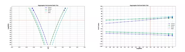
Figure 1: Superior performance at 16GT/s across all channel lengths, far exceeding the UCIe spec
In the bathtub curve in Figure 1, the phase interpolator (left, Figure 1). and Vref (right, Figure 1) eye performance at the specification requirement of 1e-15 (shown as a red dotted line) shows excellent receiver performance for short, medium, and maximum die-to-die spacing. Figure 2 shows the receiver eyes as measured using a PRBS checker, with PRBS patterns continually transmitted at max speed across the UCIe channel. The successful hardware-based bringup and training results in wide open eyes across all lanes.
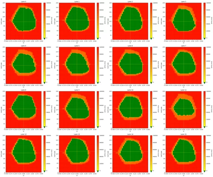
Figure 2: All lanes show wide open receive eyes with a PRBS pattern at 16GT/s
The PHY supports full duplex communication across 16 Tx and 16 Rx standard package interconnects of up to 25mm distance. We have extensively tested it under various distances and routing methods to validate performance. Our PHY, implemented on Samsung's 5nm automotive process, meets the UCIe specification and stringent automotive requirements. The PHY supports high-performance computing (HPC) applications by providing low-power, low-latency seamless communication between chiplets in a multi-chiplet design crucial to HPC/AI/ML applications.

Figure 3: Cadence is a contributing member of UCIe, where we help define specs, including automotive
The PHY is complemented by our portfolio of UCIe controllers in various configurations. We support everything from raw streaming interfaces to full PCIe protocol and lightweight, high-efficiency AXI, CXS.B, and CHI-C2C bridges. Our controller portfolio includes multiple configurations, including UCIe-CXS and UCIe-AXI, that have received ASIL-B compliance certification from SGS. The controller and PHY are seamlessly merged into an IP subsystem before delivery and extensively verified at all levels to provide an easy integration experience so customers can focus on their SoC differentiators.
We are excited to continue our collaboration with Samsung Foundry to enable our mutual customers with best-in-class IP solutions that accelerate innovation and bring the next generation of automotive and high-performance computing systems to market.
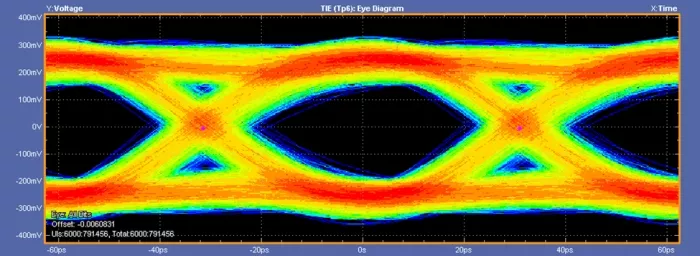
Figure 4: UCIe Tx eye at 16GT/s is shown on an oscilloscope
Learn more about Cadence's UCIe IP, and stay tuned for more updates as we push the boundaries of connectivity and system performance!
Related Semiconductor IP
- Universal Chiplet Interconnect Express (UCIe™) Controller
- Universal Chiplet Interconnect Express (UCIe™) PHY
- Simulation VIP for UCIE
- USB-C 3.1/DP TX PHY in Samsung (14nm, 11nm, 5nm)
- 32G PHY in Samsung (10nm, 8nm, 4nm, 5nm, SF2)
Related Blogs
- Cadence Tapes Out 32GT/s UCIe IP Subsystem on Samsung 4nm Technology
- Advancing Die-to-Die Connectivity: The Next-Generation UCIe IP Subsystem
- Dream Chip, Cadence Unveil Automotive SoC with Tensilica IP at embedded world '25
- The Next-Generation UCIe IP Subsystem for Advanced Package Designs
Latest Blogs
- Area, Pipelining, Integration: A Comparison of SHA-2 and SHA-3 for embedded Systems.
- Why Your Next Smartphone Needs Micro-Cooling
- Teaching AI Agents to Speak Hardware
- SOCAMM: Modernizing Data Center Memory with LPDDR6/5X
- Bridging the Gap: Why eFPGA Integration is a Managed Reality, Not a Schedule Risk