Cadence Powers AI Infra Summit '25: Memory, Interconnect, and Interface Focus
AI is driving a new semiconductor renaissance—it's no longer just a workload, but the defining force behind a new era of semiconductor innovation. Cadence Fellow Charles Alpert echoed this message in his keynote, "Design for AI and AI for Design," offering insights into how AI is reshaping infrastructure and accelerating innovation. His talk set the tone for the AI Infra Summit 2025, paving the way for the Cadence Silicon Solutions Group (SSG) to showcase its cutting-edge IP portfolio that is rearchitecting the silicon foundation of AI infrastructure.

Built on the advanced 3nm process node, Cadence's demos addressed the three pillars of AI system design: memory bandwidth, high-speed interfaces, and scalable interconnects (from Figure 1). As data centers evolve to meet the demands of increasingly complex AI models, Cadence is leading the charge with silicon-proven solutions that deliver performance, efficiency, and future-ready scalability.
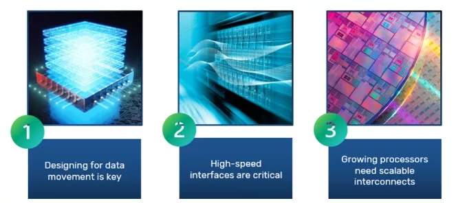
Figure 1. Cadence Continuous Innovation in Standards and Implementations
Each demo exemplifies how Cadence is solving real-world challenges in AI data centers through silicon-proven innovation.
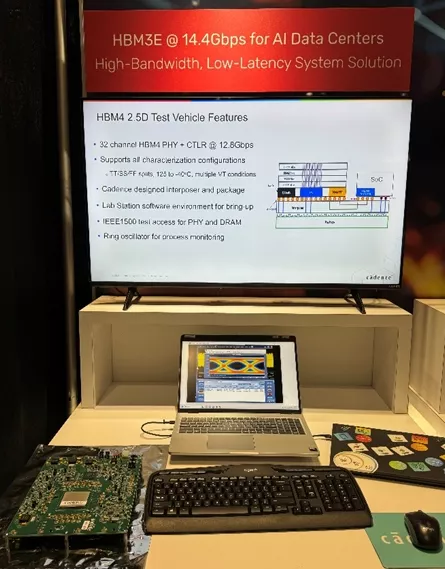
HBM3E at 14.4Gbps for AI Data Centers: High-Bandwidth, Low-Latency System Solution
In AI workloads, data movement is often the bottleneck. Cadence's HBM3E IP, operating at 14.4Gbps on the 3nm process node, is engineered to overcome this challenge by delivering high-bandwidth, low-latency memory access. The demo showcased a complete system solution with tightly integrated PHY and controller IP, enabling efficient data flow between memory and compute. This is critical for training large models and running inference at scale, where every nanosecond counts. By designing for data movement, Cadence empowers AI systems to operate faster and more efficiently.
 +
+
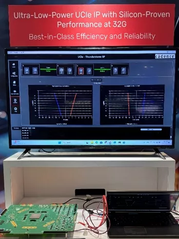
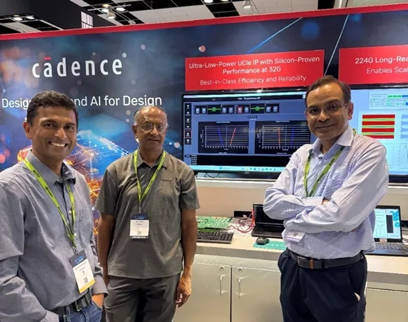
Ultra-Low-Power UCIe IP with Silicon-Proven Performance at 32G: Best-in-Class Efficiency and Reliability
As processors grow in complexity, scalable interconnects become essential to maintain performance and modularity. Cadence's UCIe IP, demonstrated at 32G in a standard package on the 3nm process node, addresses this need with ultra-low power consumption and proven reliability. The demo emphasized how chiplet-based architectures can scale compute density while maintaining energy efficiency. An advanced package version is currently under lab characterization and expected to be ready by early 2026, offering even greater integration flexibility. With scalable interconnects, Cadence empowers next-generation AI SoCs to achieve best-in-class efficiency and reliability.
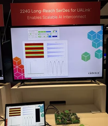
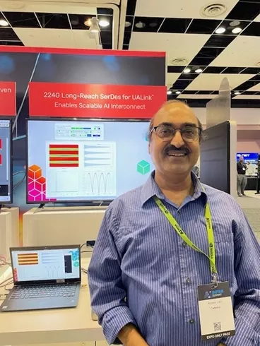
224G Long-Reach SerDes for UALink: Enables Scalable AI Interconnect
High-speed interfaces are the backbone of distributed AI systems. Built on the 3nm process node, Cadence's 224G Long-Reach SerDes IP is designed for the emerging UALink standard. At AI Infra Summit, Cadence demonstrated exceptional performance with a 45dB channel reach—well beyond the 40dB spec. This capability ensures robust, high-speed communication across racks and data center fabrics, supporting the massive data exchange required by AI accelerators. By delivering reliable, high-speed interfaces, Cadence enables scalable interconnects that keep pace with AI's growing demands.
Summary
At AI Infra Summit 2025, Cadence took center stage in solving the most demanding challenges facing AI infrastructure today. From optimizing data movement and enabling scalable chiplet architectures to advancing high-speed interconnects, our 3nm IP portfolio is engineered for the future of AI. Now, with 2nm deployments underway, Cadence is fueling the next wave of innovation—delivering the performance, efficiency, and scalability that AI leaders need to push boundaries and accelerate breakthroughs.
Learn more about Cadence key AI solutions (HBM, UCIe, UALink, and more).

Related Semiconductor IP
- High speed MACsec Engine 100G/200G/400G/800G/1.6T
- Temperature/Voltage sensors
- AMBA Bus Host to eSPI Controller/Target
- AMBA Bus Host to eSPI Controller
- AMBA Bus Host to eSPI Target
Related Blogs
- LPDDR6: A New Standard and Memory Choice for AI Data Center Applications
- UA Link vs Interlaken: What you need to know about the right protocol for AI and HPC interconnect fabrics
- Focus on Memory at AI Hardware Summit
- HBM4 Boosts Memory Performance for AI Training
Latest Blogs
- From Classical CAN and CAN FD to CAN XL: Functional Safety and Security for Next-Generation In-Vehicle Communication
- Accelerating Embedded Memory Performance with 16-bit xSPI PSRAM IP
- Why nonce reuse can break AES-GCM security in embedded systems
- PQSecure™-Agility Earns NIST CAVP Validation
- Mitigating the Single-Source Trap