Analog Design and Layout Migration automation in the AI era
The design teams typically invest years and numerous iterations to validate IP and produce a functioning chip. Once this validation is complete, they create derivatives of the silicon-proven IP, often adapting it across various process nodes (such as 7nm HPM, HPC, LPP) or transferring it to entirely new nodes (like 5nm, 6nm, or 4nm).
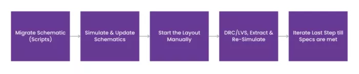
Traditionally, IP migration involves script-based schematic migration, followed by iterative checks, simulations, and edits until the design meets design specifications. Layout engineers then manually create a layout from the updated schematic, referencing the silicon-proven IP layout, and cycle through extraction, post-layout simulation, and layout updates. Here’s the traditional flow.
However, in the AI era, this structure is shifting. The AI/ML-powered automation accelerates schematic identification, layout generation, and rule-based verification, leading to shorter design cycles and reduced human intervention.
What are the disadvantages of this traditional design migration approach?
The traditional design migration approach comes with several key disadvantages. It is inherently time-consuming and resource-intensive, the migration of mid-size design often takes more than 12 weeks due to sequential tasks like 1 week for schematic migration, 3-4 weeks for simulation and updates, 5-8 weeks for manual layout, and 2-3 weeks for DRC/LVS, extraction, and re-simulation for a mid-size design. Even with parallel work, the process typically takes at least 8 to 10 weeks.
How can AI or the new design tools improve this migration process?
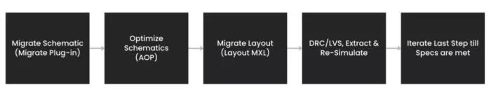
New EDA migration tools have significantly streamlined the process, with vendors claiming up to 70% improvement. For instance, Cadence Virtuoso offers a ‘Migrate’ plugin for schematic migration, an ‘Advanced Optimization Platform (AOP)’ for schematic optimization, and a ‘Migrate’ plugin in ‘Layout MXL’ for capturing and migrating layout placement and routing.
Below is a look at how the new design flows.
How effective is the ‘migrate’ plugin for schematic migration & AOP for optimization?
Schematic migration primarily requires a mapping file for CDF parameters (e.g., width, length, fingers, fins) between source and target process nodes. Foundry-provided mapping files streamline intra-foundry migrations to less than a day, while inter-foundry migrations can take 2-3 days for setup and verification. The tool intelligently handles symbol, terminal, and connectivity variations.
On the optimization side, the Advanced Optimization Platform (AOP), leveraging AI/ML, significantly reduces optimization time from 3-4 weeks to less than a week by automatically finding spec-compliant parameter combinations across various corners, with runtime depending on CPU cores. This is an improvement over the basic parametric sweep. The user needs to input the range of values and step size for a parameter, and the tool iterates over them to output the value that meets the specification. As this process is computationally intensive, the AI/ML flow can help to identify the values that meet the specifications with the fewest iterations possible.
How effective is the migration option for Layout migration?
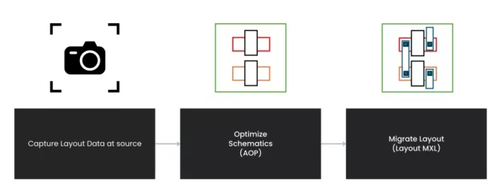
The efficacy of layout migration depends on its initial Layout XL compliance. Migration leverages a mapping file for parameters and scaling, with a source-side “Capture” step preceding target-side placement migration (from schematic) and routing migration (via Layout MXL).
Efficiency gains were 40% to 50% for “Core” layouts and 20% to 30% for “I/O” or mixed blocks, with Routing migration achieving up to 70% efficiency. Our experience with 7 nm to 5 nm, 4 nm to 5 nm, and 4 nm to 3 nm migrations shows that this method saves approximately 2 to 3 weeks.
In the worst-case scenario, the overall project time reduces from 16 weeks to 10 weeks due to migration & optimization tools. (~40-50% reduction)
In the best-case scenario, the overall project time reduces from 8-10 weeks to 5-6 weeks (~40-50% reduction)
What are the current challenges in Layout Migration? How can they be improved?
Effective layout migration hinges on Layout XL compliance, ensuring that devices, nets, and pins are correctly bound to the schematic. While automatic binding with the LVS cross-reference file could streamline this further, that feature is still in development.
Discrepancies in X/Y scaling factors between core and I/O devices often lead to misalignments requiring manual layout correction.
Via generation during routing migration is not automatic, users must regenerate them.
For hierarchical layouts, non-XL-compliant sub-blocks halt the entire capture process, indicating a need for selective block migration.
What is the ideal case scenario of migration?
In the best-case scenario, schematic migration, optimization, and layout migration would be completed with just a few clicks—delivering a fully functional layout that successfully passes post-layout simulation without manual intervention.
Looking ahead, Agentic AI could take this even further. By enabling users to issue natural language commands, the AI could interpret and execute tasks such as schematic migration, parameter optimization, layout transformation, and final tuning—automating the entire flow from design to validation with minimal user input.
As design automation advances, MosChip’s experience in analog design and layout, along with its expertise in schematic and layout migrations, positions it to support teams looking to streamline their workflows. With a strong foundation in IP porting and reusable design practices, MosChip® can help teams adapt to emerging methodologies and take full advantage of new automation possibilities.
Related Semiconductor IP
- Verification IP for C-PHY
- Band-Gap Voltage Reference with dual 2µA Current Source - X-FAB XT018
- 250nA-88μA Current Reference - X-FAB XT018-0.18μm BCD-on-SOI CMOS
- UCIe D2D Adapter & PHY Integrated IP
- Low Dropout (LDO) Regulator
Related Blogs
- Applied AI in Analog IC Design Migration
- The Integrated Design Challenge: Developing Chip, Software, and System in Unison
- UEC-LLR: The Future of Loss Recovery in Ethernet for AI and HPC
- The Hidden Threat in Analog IC Migration: Why Electromigration rules can make or break your next tapeout