A/D Converter (ADC) IP
An ADC IP (Analogue to Digital Converter) is a data converter which allows digital designs to interface with the real world by encoding an analogue signal into a binary code.
The primary function of an A/D Converter semiconductor IP is to enable seamless interaction between analog input sources and digital processing units. High-quality A/D Converters ensure accurate data capture and conversion, minimizing loss of information during the transformation process. As the demand for more precise and faster data processing increases, the importance of these IPs grows, driving innovations in resolution, sampling rates, and power efficiency.
All offers in
A/D Converter (ADC) IP
Filter
Compare
517
A/D Converter (ADC) IP
from
62
vendors
(1
-
10)
-
14-bit, 1200 MSPS Ultra Low Power ADC in 28nm CMOS
- 14-bit resolution, sampling rate up to 1200 MSPS
- Fully differential operation, fully specified from -40C to 125C
- Ultra low power dissipation
- Internal bandgap and voltage reference
-
Ultra high-performance low-power ADC
- TSMC 28nm
- Ultra high-performance low-power ADC
- 12-bit ADC resolution
- Sampling rate up to 5GSPS
-
10-bit SAR ADC - XFAB XT018
- The TS_ADC_10b_X8 is a 10-bit capacitive successive approximation register (SAR) Analog-to-Digital converter (ADC).
- It operates with a 3.3 V analog power supply, a 1.8 V digital power supply, and an external voltage reference.
- The ADC converts single-ended input voltages and requires no external S/H circuit.
-
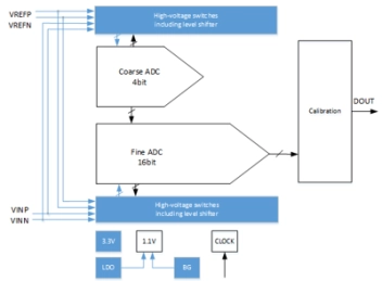
12-bit/16-bit SAR ADC
- 12 bits 100Msps SAR ADC on 28nm process;
- 12 bits 25Msps SAR ADC and Pipeline ADC above 100Msps on 40/55nm process;
- 16 bits 2/1Msps SAR ADC on 40/55nm process;
-
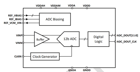
12-bit 400MSPS ADC on TSMC 7nm
- The ODT-ADS-12B2400M-7T is an ultra low power ADC designed for use in a 6/7nm CMOS process.
- This 12-bit, 400MSPS ADC supports input signals up to 200MHz and features a differential full-scale range of 1.0Vpp and excellent static and dynamic performance.
-
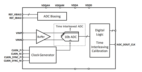
10-bit 2.5GSPS ADC
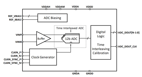
- The ODT-ADS-10B2P5G-T16 is an ultra lowpower, high-performance time-interleaved ADC designed in a 16nm CMOS process.
- This 10-bit, 2.5GSPS ADC supports input signals up to 1.0 GHz and features a differential full-scale range of 1.0Vpp with excellent static and dynamic performance.
-
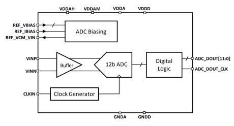
12 bit, 200 MSPS ADC on TSMC 16nm FFC
- The ODT-ADS-12B200M-16FFCT is an ultra low power ADC designed in a 16nm CMOS process.
- This 12-bit, 200MSPS ADC supports input signals up to 100MHz and features a differential full-scale range of 1.0Vpp and excellent static and dynamic performance.
-
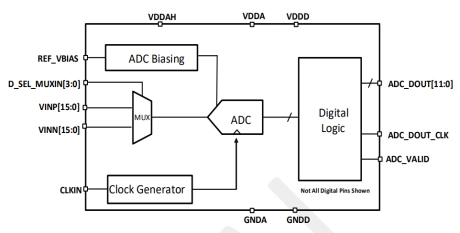
12-bit, 5 MSPS ADC with 8:1 Input Mux in a TSMC 6nm
- The ODT-ADS-12B5M-6T is an ultra-low-power, high-linearity ADC with rail-to-rail inputs designed in a TSMC 6nm process.
- This 12-bit, 5MSPS ADC supports input signals up to 1 MHz and features excellent static and dynamic performance.
- The input front-end includes a mux that can support 16 single-ended or differential inputs.
-
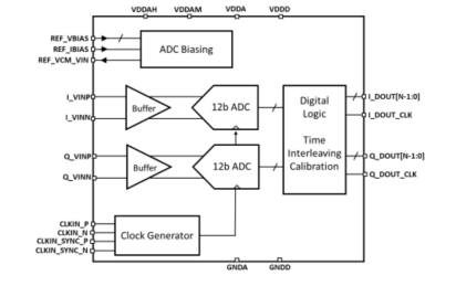
12-bit, 4 GSPS High Performance IQ ADC in GF22FDX
- GF22FDX Process
- 12-bit resolution, 4GSPS update rate
- Dual ADC configured as IQ Pair
-
12-bit, 8 GSPS ADC in 7nm CMOS
- The ODT-ADS-12B8G-7nm is an ultra-highperformance time-interleaved ADC designed in a 7nm CMOS process.
- This 12-bit, 8GSPS ADC supports input signals up to 2.5 GHz and features a differential fullscale range of 0.8Vpp and excellent static and dynamic performance.