TeraPool: A Physical Design Aware, 1024 RISC-V Cores Shared-L1-Memory Scaled-up Cluster Design with High Bandwidth Main Memory Link
By Yichao Zhang 1, Marco Bertuletti 1, Chi Zhang 1, Samuel Riedel 1, Diyou Shen 1, Bowen Wang 1, Alessandro Vanelli-Coralli 1,2 and Luca Benini 1,2
1 Integrated Systems Laboratory (IIS), ETH Zurich, Switzerland
2 Department of Electrical, Electronic and Information Engineering (DEI), University of Bologna, Italy
Abstract
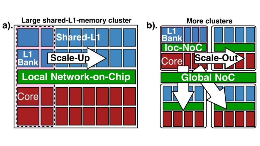
Shared L1-memory clusters of streamlined instruction processors (processing elements - PEs) are commonly used as building blocks in modern, massively parallel computing architectures (e.g. GP-GPUs). Scaling out these architectures by increasing the number of clusters incurs computational and power overhead, caused by the requirement to split and merge large data structures in chunks and move chunks across memory hierarchies via the high-latency global interconnect. Scaling up the cluster reduces buffering, copy, and synchronization overheads. However, the complexity of a fully connected cores-to-L1-memory crossbar grows quadratically with PE-count, posing a major physical implementation challenge. We present TeraPool, a physically implementable, >1000 floating-point-capable RISC-V PEs scaled-up cluster design, sharing a Multi-MegaByte >4000-banked L1 memory via a low latency hierarchical interconnect (1-7/9/11 cycles, depending on target frequency). Implemented in 12nm FinFET technology, TeraPool achieves near-gigahertz frequencies (910MHz) typical, 0.80 V/25°C. The energy-efficient hierarchical PE-to-L1-memory interconnect consumes only 9-13.5pJ for memory bank accesses, just 0.74-1.1x the cost of a FP32 FMA. A high-bandwidth main memory link is designed to manage data transfers in/out of the shared L1, sustaining transfers at the full bandwidth of an HBM2E main memory. At 910MHz, the cluster delivers up to 1.89 single precision TFLOP/s peak performance and up to 200GFLOP/s/W energy efficiency (at a high IPC/PE of 0.8 on average) in benchmark kernels, demonstrating the feasibility of scaling a shared-L1 cluster to a thousand PEs, four times the PE count of the largest clusters reported in literature.
Index Terms — Manycore, RISC-V, Scalability, Physical Design Aware
To read the full article, click here
Related Semiconductor IP
- Low Dropout (LDO) Regulator
- 16-Bit xSPI PSRAM PHY
- ASIL B Compliant MIPI CSI-2 CSE2 Security Module
- SHA-256 Secure Hash Algorithm IP Core
- EdDSA Curve25519 signature generation engine
Related Articles
- VLSI Physical Design Methodology for ASIC Development with a Flavor of IP Hardening
- Optimize SoC Design with a Network-on-Chip Strategy
- Design and implementation of a hardened cryptographic coprocessor for a RISC-V 128-bit core
- Get More Reliable Automotive ICs with a Shift Left Design Approach
Latest Articles
- A 129FPS Full HD Real-Time Accelerator for 3D Gaussian Splatting
- SkipOPU: An FPGA-based Overlay Processor for Large Language Models with Dynamically Allocated Computation
- TensorPool: A 3D-Stacked 8.4TFLOPS/4.3W Many-Core Domain-Specific Processor for AI-Native Radio Access Networks
- Assertain: Automated Security Assertion Generation Using Large Language Models
- VolTune: A Fine-Grained Runtime Voltage Control Architecture for FPGA Systems