Simplifying SoC design with the Customizable Control Processor
Abstract :
With the circuit density available in today’s ASIC designs, increased integration can complicate the design of a system-on-a-chip (SoC). IBM’s Customizable Control Processor addresses the challenges facing design engineers by identifying the common features required in most SoC designs, and creating a hardened platform that can be used as a starting point for new designs. With a processor subsystem that has already been integrated, verified and timed to package I/O, the design team can focus their efforts on product differentiation. This approach improves design cycle time by addressing the critical path of the design flow, which includes the architecture, integration, verification, physical design and timing. In addition, standardization of the processor complex enables the reuse of software, and concurrent hardware and software development.
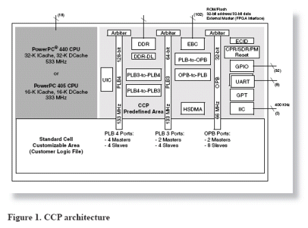
This paper describes the architecture of the IBM Customizable Control Processor (CCP), shown in Figure 1. It also describes the design and verification methodologies used to develop an SoC with the CCP.
Introduction
Several new platform-based design approaches attempt to address the growing complexity and increasing development cost of new SoC designs. One such approach, structured ASICs, predefines much of the content for a target application, with customization available only in the final levels of metal. This approach enables manufacturing efficiencies, and only requires a few new masks for each design. However, structured ASICs limit the choices designers can make to differentiate their product. In addition, the predefined features occupy silicon whether required by the design or not; this adds to the product cost.
Field programmable gate array (FPGA) manufacturers offer another approach. They provide a hardened processor, combined with selected intellectual property (IP), and a section of embedded FPGA for custom logic. This approach limits customization to the embedded FPGA section, which consumes a significant silicon area for a limited amount of unique customer logic. The unit cost is higher than the cost of the equivalent logic function in an ASIC. However, minimal non-recurring expense is required.
As another alternative, discrete components such as a control processor and an FPGA can be used. This approach also has limitations. FPGAs do not offer the same performance and density that a standard cell ASIC can achieve, and FPGAs can be expensive. Due to the inefficiencies of FPGA architecture, large logic circuits require partitioning of the design. Large FPGAs are now available, but they may be too costly for production volumes and are primarily used for prototyping.
Designers often use ASIC SoCs for high-volume, cost-sensitive applications because they can be optimized for maximum content in the smallest die size. While a standard cell ASIC SoC approach provides optimal performance at a low unit cost, the up-front nonrecurring expense and a longer development cycle can be deterrents.
The CCP combines the strengths of each approach, resulting in a hybrid solution that provides an optimum balance between a standard product and a custom SoC. Like a standard product, the hardened processor subsystem is already placed, wired and timed. In addition, the CCP reserves a section of the image for customization. This preserves the flexibility of an ASIC design and provides an opportunity for maximum product differentiation. Because all levels are customizable and an ASIC standard cell methodology is used, the designer can use IBM Blue Logic® cores, third-party IP, compilable macros, and all elements of the ASIC library including embedded memory. A major advantage provided by the CCP is that it enables the reuse of those components that are common to multiple applications.
Architecture
Figure 2 shows the floorplan of the CCP, which is a hardened (preplaced and prewired) version of an IBM PowerPC® SoC. The predefined area of the chip contains cores and features found in most control and communication applications. The custom area of the chip (the white space) allows each application of the CCP to be personalized with cores from the IBM core library, third party IP, embedded memory or unique logic implemented in IBM ASIC standard cells. There are 263 preassigned I/Os for the hardened portion of the chip; 177 I/Os are available in the custom area to tailor the SoC for a specific design.
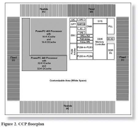
Each chip consists of three regions: the processor area, the CCP predefined area and the customizable area. The processor area supports a PowerPC 440 or PowerPC 405 processor. The PowerPC 440 processor has a target frequency of 533 MHz, while the PowerPC 405 processor has a target frequency of 333 MHz. The CCP predefined area includes a double data rate (DDR) memory controller, direct memory access (DMA), timers, I/O ports and an assortment of serial interfaces. The customizable area is the region of the chip that can be populated with IBM ASIC standard cell devices. This customizable area can be configured with 2.1 M gates of logic when a PowerPC 440 processor is used; 3 M gates of customizable area are available with a PowerPC 405 processor. Alternative configurations include the integration of logic and embedded memory in the customizable area. Both embedded static random-access memory (SRAM) and embedded dynamic random-access memory (DRAM) are supported.
PowerPC processor area
The processor area in the CCP chip supports either a hardened PowerPC 440 or 405 CPU with the following features:
| PowerPC 440 Processor | PowerPC 405 Processor | |
| Target Frequency (MHz) | 533 | 333 |
| Instruction Cache (KB) | 32 | 16 |
| Data Cache (KB) | 32 | 16 |
| Debug Interfaces | RISCTrace and RISCWatch | |
CCP predefined area
The CCP predefined area is a collection of integrated cores common to most SoC designs. The predefinition of the architecture, including the placement of peripheral cores, wiring and timing, allows for shorter development time and, consequently, lower development cost.
The CCP predefined area features:
- Microprocessor interface for PowerPC 440 or PowerPC 405 processor
- Processor local bus (PLB) version 4
- 133-MHz target frequency
- 128-bit read and write data buses
- • PLB version 3
- 133-MHz target frequency
- 64-bit read and write data buses
- PLB 4-to-PLB 3 bridge
- PLB 3-to-PLB 4 bridge
- DDR memory controller to PLB4
- Support for DDR200, DDR266
- 32-bit or 40-bit data bus
- 13-bit address bus
- Optional 64-bit or 72-bit data bus, supported with customizable I/O
- 8-bit error correction code (ECC) support
- Two banks of DDR memory
- External bus controller to PLB3 (EBC to PLB3)
- Support for 8-, 16- or 32-bit byte-addressable bus width
- Byte parity on data bus
- 32-bit address bus
- EBC-to-CoreConnect™ for FPGA rapid prototyping
- Support for up to eight banks of read-only memory (ROM), erasable programmable ROM (EPROM), SRAM, flash memory and slave peripheral I/O <>>
- External master support with mastering on external bus or PLB
- Direct memory access to PLB3 (DMA to PLB3)
- Four channels for internal peripherals and memory-to-memory moves
- Four external DMA channels
- Scatter/gather capability
- On-chip peripheral bus (OPB) version 1.9
- 32 bits
- 66-MHz target frequency
- Two National Semiconductor 16750-compatible universal asynchronous receiver transmitters (UARTs) <>>
- Inter-integrated circuit (I2C) interface with inte grated, 5-V tolerant bus transceivers
- One general-purpose I/O (GPIO)
- Multiplexed I/O functions
- Universal interrupt controller (UIC)
- Support for internal and external interrupts
- General-purpose timers/variable frequency generator (GPTVFG)
- Three capture timers
- Four compare timers
- Four variable-frequency generators
- One countdown timer
- Clock and power management (PM) control logic
- Single standard phase-locked loop (PLL) for system-clock generation
- 33- to 66-MHz PLL reference-clock range
- Integral-mode clock generation supports 1:1, 1:2, 1:3 and 1:4 CPU-to-PLB clock ratios
- Non-integral (n/m) mode clock generation supports 4:3, 5:3, 7:3 and 5:2 CPU-to-PLB ratios <>>
- Integral-mode clock generation supports 1:2, 1:3, 1:4 and 1:5 PLB-to-external-clock ratios
- Class 1 PM: unconditional sleep for general-purpose timer (GPT), UIC, GPIO and UART
- Class 2 PM: macro-paced sleep for EBC, high-speed PLB memory controller (HSPLBMC), PLB arbiter, PLB-to-OPB bridge, high-speed DMA driver (HSDMA) and PowerPC 440 or PowerPC 405 processor
- Class 3 PM: clock power management (CPM) and macro-paced sleep for I2C
- Wake from sleep capability for CPU
- IBM level-sensitive scan design (LSSD) manu facturing test compliant
- IBM boundary scan
- Institute of Electrical and Electronics Engineers (IEEE®) 1149.1 Joint Test Action Group
- (JTAG) boundary scan
- Second test access port (TAP) controller supports additional JTAG instruc tions
CCP customizable area
The customizable area allows for standard cell implementations of additional logic to tailor the CCP for application-specific needs. There is enough room in this area for approximately 2.1 M logic gates with the PowerPC 440 processor or for 3 M logic gates with the PowerPC 405 processor.
Clocking extensions are prewired into the customizable area of the chip. All clocks associated with the CCP are brought into the customizable area high in the clock tree to allow a relatively deep clock tree that is balanced with the hardened portion of the CCP.
- All unassigned interrupts from the UIC are prewired into the customizable area to allow for the wiring of custom, internally initiated interrupts or of external interrupts.
- All unused power-management register bits are prewired into the custom area to allow power management of custom cores and macros.
- The system DCR registers (SDR) core addressing is extended into the custom area to allow more control registers from the custom area into this address space.
- The 64-bit, 133-MHz PLB3 bus has two master ports and four slave ports.
- The 128-bit, 133-MHz PLB4 bus has four master ports and four slave ports.
- The CCP OPB is extended into the customizable area to allow up to two OPB masters and eight OPB slaves.
- There are 177 flexible I/Os in the custom area, to allow for the customization of I/O type as well as I/O placement.
- The device control register (DCR) is pre-wired into the custom area to allow additional control registers into this address space.
Most of the SoC on the CCP platform is already developed, with the exception of the customer logic. Thus, the developers start with a model of the entire chip (the chip-top structure). At this point, the developers can start simulating test cases and running system software. The developers then tailor the customer logic file (CLF), creating an optimized design for their unique application. Figure 3 shows the design hierarchy and how the CLF fits into the design.
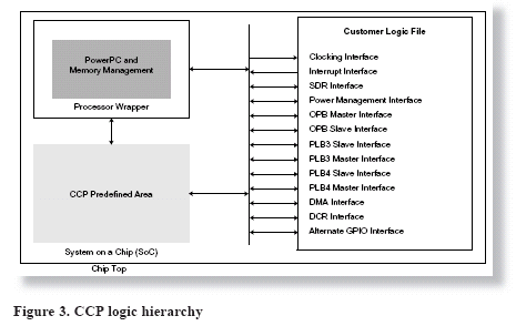
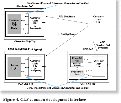
Figure 4 shows how the CLF file can be instantiated into a high-level simulation environment, or into an FPGA emulation or prototyping environment, and finally used in the chip itself. To simplify the verification requirements after the customizable logic is tailored and returned, the CLF is instantiated into a known, untouched and preverified chip-top structure. After typical IBM ASIC front-end processing, the logic in the CLF is placed and wired in the unused white space of the CCP. All other logic has been preplaced, prewired and pretimed.
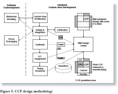
The CCP design methodology consists of the hardware and software flows shown in Figure 5.
Hardware methodology
The hardware methodology flow begins with the architectural definition of the CCP custom area and the selection of the IP. Next, the design and integration phase implements the logic design in the Verilog hardware description language (HDL) by attaching the IP to standard CCP CoreConnect ports. The IP can be from the IBM portfolio, provided by a third party or provided by the customer. After the HDL design has been integrated, both the verification phase and logic synthesis phase can begin. The goal of verification is to validate the interconnection of the IP to the CCP framework. The goal of the ASIC standard cell synthesis phase is to create a netlist of only the custom area to hand off to the IBM Design Center.
In the I/O assignment phase, the customer must select the specific I/Os needed for the custom area, and perform Simulation Program with Integrated Circuit Emphasis (SPICE) analysis if necessary. In the timing phase, timing assertions for the custom area logic are created. These inputs let the IBM Design Center handle the remaining integration of the netlist into the CCP framework, microprocessor integration, manufacturing test, physical design, assignment of the remaining personalized I/Os and release of the design to manufacturing.
Software methodology
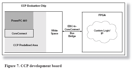
On the software side, early software development can begin on two fronts. First, both software development and architectural analysis take place using a behavioral model that describes the CCP core and the surrounding test bench. The behavioral model supports C/C++, SystemC and RTL (or any combination). Second, software development can take place on an FPGA-based rapid prototyping platform (the CCP development board) that uses a CCP evaluation chip. With the CCP development board, software can execute at more real-world speeds via a cycle-accurate CoreConnect bridge on the CCP development board.
Verification and simulation
The intent of the verification methodology is to provide chip architects, designers and software developers with the tools required for early software development and hardware verification, as well as an environment that allows continuous design refinement and verification. This requires a heterogeneous simulation environment that allows designers to simulate software and hardware in a range of abstraction levels, communicating through industry-standard interfaces.
Hardware and software comodeling and coverification
Figure 6 illustrates the verification environment. The core of the system is a cosimulation engine, called IC-Sim for in-circuit simulation, whose function is to interpret the various requests issued by the component models and translate them into the right level of abstraction for the model invoked.
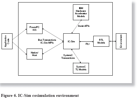
Software is developed using either an instruction set simulator (the IBM PowerPC ISS) or native code on the host computer. The ISS (or special functions in native code on the host) traps the bus transactions. They are passed to the IC-Sim engine by calling the IC-Sim model programming interface (MPI). The IC-Sim engine translates the bus requests from the software side to bus requests on the hardware side (that is, to the hardware components).
The hardware components can be modeled in three main abstraction levels:
- SystemC transaction-level models (TLMs)
- Register transfer level (RTL) (Verilog, or very high-speed, integratedcircuit, hardware-description language [VHDL])
- IBM hardware accelerator model.
If the hardware component is in the SystemC TLM, the IC-Sim calls the appropriate transaction-level methods as defined by the bus TLM. If the hardware component is in the RTL, the IC-Sim translates the bus request into the correct signal values for the RTL pins. The IC-Sim then passes the signal values by using the RTL-simulator programming-language interface (PLI). Any vendor simulator that uses industry-standard PLI can be used. A similar approach is used for the hardware accelerator. Using this environment, designers can seamlessly interchange model types to suit different phases of development activities.
The environment includes the PowerPC 405/440 ISS and the RISCWatch debugger. RISCWatch provides consistent debug interfaces during presilicon, rapid prototyping and hardware bring up. It also includes the ability to test basic functionality and component connectivity using the IBM test operating system (TOS), which provides the initial system interconnection and basic hardware bring-up testing.
IC-Sim adapter architecture
The IC-Sim considers the CPU (represented by the ISS or native code on the host) and the component models as clients. Clients can interact with the bus through the IC-Sim MPI. The CPU client accesses the bus through load and store instructions, and responds to exceptions and interrupts, all through calls to IC-Sim MPIs. The MPI interface allows single beat and burst transactions. Clients are connected using sockets, shared-memory interprocess communication IPC or a dynamic link library (DLL).
The default timing accuracy of the IC-Sim engine follows the accuracy of the model simulated. When adapting to RTL event simulators, accuracy is at the RTL clocks with no loss of performance. When using the IBM hardware accelerator, trade-offs maximize the efficiency of the accelerator, and the default accuracy is at the transaction boundary. When interfacing to SystemC TLM, accuracy is at the transaction level. Users can override the defaults to trade off cycle accuracy at the expense of simulation performance. For example, software debugging is likely to need less cycle accuracy than hardware development.
CCP virtual board
The CCP hardware platform is modeled in the IC-Sim environment as a virtual board, which consists of a combination of behavioral models and is conceptually equivalent to the CCP development board. Test bench models provide the realworld, complex stimulus of chip I/O that is essential for meaningful software development and system-level verification. The virtual board enables designers to quickly create their value-add IP as simulation models and integrate them with the CCP. Designers can begin very early analysis, verification and software development, possibly months before hardware is available. IBM TOS diagnostic programs execute on the virtual board so users can easily integrate and check their custom logic within the system context. Because the virtual board is a simulation model, very high visibility is achieved during initial verification and device-driver and software-application development. Using the virtual board with the native execution mode of IC-Sim enhances algorithm development. The virtual board contains models for all cores in the CCP platform, integrated in the IC-Sim environment. The PowerPC ISS is used in place of the processor. Verification software, diagnostics, device drivers and applications run in the IC-Sim environment.
As the CCP development board and CCP virtual board provide the same development environment, it is easy to move from the virtual board to a rapid prototyping FPGA. Both boards provide the same code-debugging interface using RISCWatch.
Prototyping and software development
Several options facilitate system development, and enable hardware and software codevelopment. Many of the IP cores used in the CCP predefined area are the same as those used in IBM PowerPC standard products; thus, IBM PowerPC standard products can be used for system prototyping and software development. An example of such a standard product is the PowerPC 440GX processor, which is manufactured using the same process technology as the CCP. In addition to standard products, the CCP development board shown in Figure 7 is part of the CCP enablement strategy. By combining a CCP evaluation chip that includes the base CCP architecture, IP common for networking applications in the white space and a discrete FPGA, early software development and system integration are possible. The FPGA is accessed via the EBC bus and a bridge supplied by IBM. The EBC-to-CoreConnect bus bridge enables CoreConnect interface development. A JTAG interface enables the use of RISCWatch or other JTAGcompatible debuggers, and the use of a RISCTrace connector for real-time trace.
Summary
While standard products can be purchased off the shelf, often they either do not meet all the IP requirements for a specific design, or they provide unnecessary functions at an additional cost. In contrast, a custom SoC can require significant up-front investment in time and resources. The CCP approach lets you create exactly the design you envision. Because the processor superstructure is preplaced, preverified and pretimed to package I/O, the development investment is limited to application-specific content. The CCP is particularly suitable for applications that require an embedded controller, product lines with similar functions and fields with fast-paced engineering standard definitions. The CCP is also well-suited to consumer electronic applications such as printers, digital TVs, imaging and games.
Related Semiconductor IP
- NPU IP Core for Mobile
- NPU IP Core for Edge
- Specialized Video Processing NPU IP
- HYPERBUS™ Memory Controller
- AV1 Video Encoder IP
Related White Papers
- Simplifying SoC Verification by communicating between HVL Env and processor
- EDA in the Cloud Will be Key to Rapid Innovative SoC Design
- Optimize SoC Design with a Network-on-Chip Strategy
- Streamlining SoC Integration With the Power of Automation
Latest White Papers
- Ramping Up Open-Source RISC-V Cores: Assessing the Energy Efficiency of Superscalar, Out-of-Order Execution
- Transition Fixes in 3nm Multi-Voltage SoC Design
- CXL Topology-Aware and Expander-Driven Prefetching: Unlocking SSD Performance
- Breaking the Memory Bandwidth Boundary. GDDR7 IP Design Challenges & Solutions
- Automating NoC Design to Tackle Rising SoC Complexity