A 24 Processors System on Chip FPGA Design with Network on Chip
By Zhoukun WANG and Omar HAMMAMI, ENSTA ParisTech
Paris, France
Abstract :
In this paper we present a single FPGA chip implementation of a NOC based shared memory multiprocessor system with 24 processors connected to a main memory composed of 4 DDR2 banks. All the processors and DDR2 memories are connected to a NOC through Open Core Protocol (OCP-IP) interface. The MPSOC have been validated and evaluated through actual execution with matrix multiplication application. A Global Asynchronous Local Synchronous (GALS) design methodology have been adopted throughout the design cycle and exploited for clock trees designs.
I. Introduction
To reduce the pressure of time-to-market and tackle the increasing complexity of SoC, the need of fast prototyping and testing is growing [1]. Taking advantage of deep submicron technology, modern FPGAs provide a fast and low-cost prototyping with large logic resources and high performance. As Multiprocessor Systems-on-Chip (MPSoCs) [2] are strongly emerging for implementing embedded systems, the conventional interconnecting modes, such as buses and crossbars, cannot satisfy MPSOC’s requirements of performance, area as well as scalability and reliability. Network On-Chip (NOC) [3] has been proposed as a systematic approach to deal with the communication-centric design challenge. Modular structure of NoC makes multiprocessor architecture scalable and improves reliability and operation frequency of on chip modules. Furthermore the NoC approach offers matchless opportunities for implementing Globally Asynchronous, Locally Synchronous (GALS) design, which make clock distribution and timing closure problems more manageable.
In this paper we present a NOC based shared memory multiprocessor system with 24 Processing Elements (PEs) and four DDR2 memory banks. All the PEs and memory controllers are connected with a scalable NOC developed with Arteris Danube library[7].
The rest of paper is organized as follow. In section II, we will introduce the overall architecture, detail of PE and NOC connection. Section III will discuss GALS clock strategy. The results of evaluation and implementation will be shown in section IV. Related work on multiprocessor on chip is described Section V. Finally, we will conclude in Section VI.
II. Architecture
A. Overall Architecture
We target a shared memory multiprocessor architecture with 4 external memory banks (M) and 24 processor element (P) connected through 2 network-on-chip: (1) request network (2) response network.
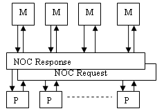
Fig.1 Shared Memory Multiprocessor with Request and Response Network-on-Chip
The IOs are not described as this is a parametrizable element of the architecture.
Our IP base design will be based on Xilinx IP for the embedded processor [10], Arteris Danube Library for NOC IPs [5, 6, 7] and custom designed IPs for OCP-IP compliant interfaces [4]. The block diagram of the overall multiprocessor architecture is illustrated in Fig.2. The multiprocessor system comprises 24 Processing Elements (PE), which can independently run their own program code and operating system. These MicroBlaze processor based PEs are connected to switches through OCP-to-NTTP Network Interface Units (NI). The OCP-to-NTTP NI, or called Master NI, translates OCP to our NOC protocol: Arteris NoC Transaction and Transport Protocol (NTTP). The switching system is connected to four NTTP-to-OCP NIs (Slave NI), which in turn connect to the respective DDR2 memory controller. Each DDR2 controller controls an off-chip DDR2 memory bank (256Mbytes).
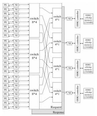
Fig.2 Block diagram of overall architecture
B. Processing Element
To increase the compatibility and to ease the reutilization of the architecture, the OCP-IP standard is used for the connection of PEs and NOC. Benefiting from the OCP standard, any processor with OCP interface can be easily connected on our system. The MicroBlaze based computing system is integrated as a PE in our FPGA design.
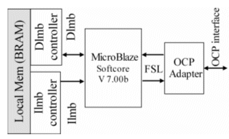
Fig.3 MicroBlaze based Processing Element
The Xilinx processing soft-core MicroBlaze V7.00 [10] is a 32bit reduced instruction set computer (RISC) optimized for implementation in Xilinx Field Programmable Gate Array (FPGA), and MicroBlaze processor IP and its memory connecting IPs are provided in the library of our FPGA design environment: Xilinx Embedded Development Kit (EDK) [10]. The MicroBlaze processor is implemented with Harvard memory architecture; instruction and data accesses are done in separate address spaces and it is highly configurable. A set of parameters can be configured at design time to fit design requirement, such as number of pipeline stages, cache size, interfaces and execution units like: selectable Barrel Shifter (BS), Floating Point Unit (FPU), hardware divider (HWD), hardware multiplier (HWM), Memory Management Unit (MMU). The performance and the maximum execution frequency vary depending on processor configuration. For its communication purposes, MicroBlaze v7.00 offers a Processor Local Bus (PLB) interface and up to 16 Fast Simplex Link (FSL) interfaces which is a point to point FIFO-based communication channel. As shown in Fig.3, the MicroBlaze is connected to its Instruction side Local Memory Bus (ILMB) controller and Data side Local Memory Bus (DLMB) controller through ILMB and DLMB respectively. Two memory controllers control 32KByte BRAM based local on-chip memory. As OCP interface is not provided by MicroBlaze, an OCP adapter, which can translate FSL interface to OCP interface have been designed and integrated in PE subsystem for the connection to the NOC.
C. NOC
Our Network On-Chip connection system is developed with the NoCcompiler and the Danube library from the Arteris [4,5,6]. The NOC is composed of a request part and a response part, and the request and response transactions are exchanged between Master NI and Slave NI. The NOC protocol, NTTP, is a three-layered approach comprising transaction, transport and physical layers. NTTP uses the packet-based wormhole scheduling technique. As shown in Fig.4, the request packets are composed of three different cells: (1) a header cell, (2) a necker cell and possibly one or more (3) data cells.

Fig.4 NTTP request packet and response packet
The header cells contain information relative to routing, payload size, packet type, and the packet target address. The necker cell provides detailed addressing information of the target. The necker cell is not needed in response packet.
The transaction layer is compatible with bus-based transaction protocol implemented in NIs. NI translates third-party protocols to NTTP at the boundary of NoC. We used OCP-to-NTTP NIs to convert OCP 2.2 protocol to NTTP protocol. The OCP basic signals, burst extensions signals and “MFlag” signal are used, as listed in Table1. The data width of MData and SDatae are 64bits. The OCP initiator can optionally associate a pressure level to requests in order to indicate service priorities at arbitration points. The pressure-level is passed to the NoC via the “MFlag” input signal, and applies to the “Pressure” field in the packet header cell, as well as the “press” signals in the physical link layer. The locked synchronization is support in our NOC. OCP initiator can use the ReadExcusive (ReadEX) command and Write or WriteNonpost command to perform a read-modify-write atomic transaction. NI sends a Lock request packet when it receives the ReadEX command. The Lock request locks the path from OCP master to the OCP slave. During the locked period, the other Masters cannot access the locked slave until the OCP master that requested ReadEX send Write or WriteNonPost command to unlock the path.
TABLE 1: The signals for the implemented OCP interface
| Function | ||
| MCmd | master Transfer command | basic |
| MAddr | master Transfer address | basic |
| MBurstLen | master Burst length | burst |
| MData | master Write data | basic |
| MDataValid | master Write data valid | basic |
| MDataLast | master Last write data in burst | burst |
| MRespAcc | master accepts response | basic |
| MFlag | master flag for pressure level | press |
| SCmdAcc | Slave accepts transfer | basic |
| SDataAcc | Slave accepts write data | basic |
| SResp | slave Transfer response | basic |
| SData | slave Read data | basic |
| SRespLast | slave Last response in burst | burst |
As shown in Fig.2, the NOC is a cascading multistage interconnection network (MIN), which contains 8 switches for request as well as 8 switches for response. 24 OCP-to-NTTP NIs and 4 NTTP-to-OCP NIs are integrated at the boundary of NOC. The OCP-to-NTTP NI converts the OCP master interface to NTTP interface and connects PE to first stage switches. First stage switches are comprised of three 8*4 switches, while the second stage contains four 3*1 switches. Each output port of switch in second stage is connected to a NTTP-to-OCP NI, which in turn connects to DDR2 memory controller.
III. Bi-Synchronous FIFO in GALS architecture
To improve the performance and reduce the power consumption of system, the GALS approach is adopted by using Bi-Synchronization method in our design. The GALS approach has been proposed to solve the timing closure problem in deep sub-micron processes by partitioning the SoC into isolated synchronous subsystems that hold own independent frequency.
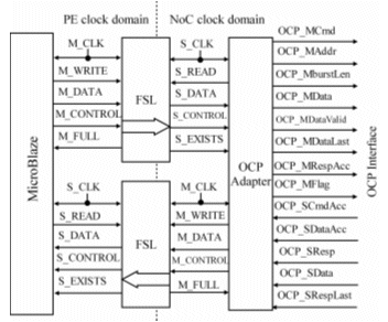
Fig.5 Block diagram of OCP adapter
To tackle the communication issue between two different clock domains, The Bi-synchronous FSL has been integrated between MicroBlaze and OCP Adapter (shown in Fig 5). The FIFO based Bi-synchronous FSL [10] makes PE and NOC as isolated synchronous islands with independent clock frequencies. Each Bi-synchronous FIFO has 2 clock inputs: M_CLK and S_CLK. The master of FSL operates at the frequency of M_CLK, while the slave of FSL runs at the frequency of S_CLK. In our FPGA design, on chip Virtex-4 Xilinx Digital Clock Managers (DCM) [9] generate different frequencies for each clock island. Thus each PE and NOC run at their own clock frequencies which eases the clock distribution problem and reduces the length of clock signal.
IV. Implementation and Performance Evaluation
A. Implementation
The whole multiprocessor system have been implemented on Xilinx FPGA Virtex-4 FX140 device [9] and Alpha-Data FPGA platform card ADPe-XRC-4 [8]. The ADPe-XRC-4 is a high performance reconfigurable PCI express board based on the Virtex-4 FX140 including 1 GByte DDR2 SDRAM in 4 independent banks and programmable Clock generator. The multiprocessor have been synthesized, place dand routed with Xilinx ISE [11] tool. The resulting floorplan is shown in Fig. 6.
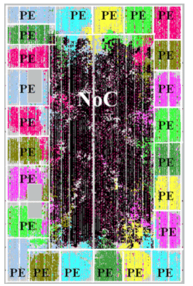
Fig.6 Floorplan of 24 PE SoC on Xilinx Virtex4FX140
The percentage of FPGA resource utilization is presented in Table2.
TABLE 2: FPGA resource utilization
| Resource | Number | Percentage |
| RAMB16s | 384 /552 | 69% |
| DSP48s | 72 / 192 | 37% |
| Slices | 55266 / 63168 | 87% |
Clearly it is possible to add hardware accelerators in order to exploit the remaining 13% of slices and 63% of the DSP48. In addition local memories and cache memories can be extended to exploit the remaining 31% of RAMB16s. This allows customization of the multiprocessor platforms to various needs. It should be noted as well that both hardcore PPC405 on the Virtex-4 FX140 have not been used and could be obviously used with little extra design effort for additional customization.
B. Performance Evaluation
For the evaluation of our NOC based MPSoC platform, we chose the matrix multiplication as our evaluating target, which is wildly used in scientific application. Due to its large multi-dimensional data array, it is extremely demanding in computation power and meanwhile it is potential to achieve its best performance in a parallel architecture. We used a course-grained parallel algorithm. We suppose that A is an M*K matrix, B is a K*N matrix, and the result C is an M*N matrix. In the phase of task dispatch, A is partitioned into M/b1 blocks, where b1 indicates the buffer size of each processing element for the first matrix, i.e. each PE can buffer b rows of K elements at each iteration. If M cannot be divided by b evenly, the last block contains the remaining rows which are less than b. In same fashion, B is partitioned into N/b2 blocks, where b2 indicates the buffer size within each node for the second matrix. After this partitioning is done, each calculating node works with the blocks from A corresponding to its node number, i.e. the nth node works on the bth block where (b mod n = P) (P: Total number of processing elements.) and the entire B. So at each iteration, it reads in the one block of A, which is then multiplied with all the blocks of B, resulting in a b1 * N partial result matrix. The partial result is first stored in the result buffer of each node and is stored in the corresponding memory location (according to the row number, the column is complete) before the start of the following iteration.
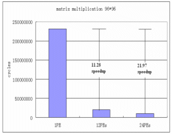
Fig.7 Evaluation of platform with 96*96 matrix multiplication application
We take the size of matrix A as 96*96, while the size of matrix B is 96*96. Both of buffer size b1 and b2 equal 4, thus when all 24 PEs work in parallel, the matrix A and matrix B can be partitioned into 24 blocks. As shown in Fig. 7, we use different number of PEs to do this matrix multiplication. The speedup of 12 PEs is 11.28 in comparison with single PE, while the speedup of 24 PEs is 22.
V. Related work
Multiprocessors System on Chips are strongly emerging and several products or ongoing R&D projects are tackling the issues related to multiprocessors [12-22].
Table 3 provides a few examples of commercial multicore implementations. They can be globally divided in 2 categories: (1) general purpose (2) application specific. In the first category we can place the ARM ARM11MPcore [13], the MIPS MIPS32 1004 Core [14] and the Renesas/Hitachi SH-X3 [15]. In the second category we can place Texas Instruments TMS320C6474/TMS320VC5441 DSP [18, 19], Freescale QorIQ P4080 [20] and the Toshiba Venezia multicore [21]. Other worth noting are Ambric [16], MAPS-TCT [22] and [12].
TABLE 3: Multicore Implementation
| MPSOC | Part | Com | PE nbr |
| ARM | ARM11 | Shared Bus | 4 |
| Texas Instruments | TMS320C6474 | Switch Central Resource | 3 |
| Texas Instruments | TMS320VC5441 | Shared Bus/HPI | 4 |
| Freescale | QorIQ™ P4080 | Corenet Coherency fabric | 8 |
| MIPS | 1004K™ Core | Coherence Manager | 4 |
| Toshiba | Venezia EX | Bus | 8 |
The ARM11 MPcore [13] is a classical shared memory 4 processors based multiprocessor based on a shared bus architecture with a snoopy cache coherency protocol (MESI). The MIPS32 1004 [14] is a 1 to 4 multi-threaded "base" cores (up to 8 hardware threads) with Coherence Management (CM) unit - the system "glue" for managing coherent operation between cores and I/O, I/O Coherence Unit (IOCU) - hardware block for offloading I/O coherence from software implementation on CPUs. Several multicore architectures are proposed by Texas Instruments [17]. The Texas Instruments TMS320C6474 [18] is a 3 DSP based multicore architecture with switch central resource (SRC) as the interconnection between the 3 DSP and the memories. The 6474 device contains 2 switch fabrics through which masters and slaves communicate: (1) data switch (2) configuration switch. The data switch fabric is a high-throughput intreconnect mainly used to move data across the system and connects masters to slaves via 128-bits data buses (SCR B) and 64-bit data buses (SCR A). The configuration switch is used to access peripheral registers. The Texas Instruments TMS320VC5441 [19] is a 4 core multicore with shared bus between 2 cores and HPI for external accesses. The Freescale QorIQ™ P4080 [17] is an 8 core multicore architecture with a Corenet coherency fabric. Each core is a high-performance Power Architecture e500mc cores, each with a 32-KByte Instruction and Data L1 Cache and a private 128-KByte L2 Cache. The CoreNet fabric is Freescale’s next generation front-side interconnect standard for multicore products. CoreNet is presented as a highly concurrent fully cache coherent multi-ported fabric. CoreNet’s point-to-point connectivity with flexible protocol architcture allows for pipelined interconnection between CPUs, platform caches, memory controllers. No details are available. Finally Toshiba proposes the Venezia architecture [21]. Our work differs from all the previously described work by a larger number of processors of smaller size emphasizing the choice of coarse grain concurrency over fine grain concurrency exploited by more sophisticated processors (VLIW e.g. MEP). It remains that we are working on architectural support for fine grained parallelism [23] through SIMD coprocessing.
VI. Conclusion
Multiprocessor System on Chip (MPSOC) are strongly emerging as best candidates for complex embedded applications. In this paper we presented a single FPGA implementation of a NOC-based 24 processors shared memory MPSOC system. IP reuse has been intensive based on various specialized IP libraries (processor, NOC) with OCP-IP interfaces for quick plug-in. First performance evaluations of this MPSOC have been conducted through a parallel code of the matrix multiplication on our multiprocessor platform which achieved a 22 speedup on the 24 processors system in comparison with single processor platform.
Future work will include more parallel applications (software defined radio, cognitive radio, image, video, military) as well as selected HLS based coprocessing on the platform.
Acknowledgement
We wish to thank Arteris support team for their kind support and their good and efficient collaboration. All trademarks are property of their respective owners.
References
1. ITRS
2. A.A. Jerraya and Wayne Wolf, “Multiprocessor Systems-on-Chip”, Morgan Kaufman Pub, 2004
3. Benini, L. ; De Micheli, G., “Networks on Chips: Technology and Tools”, Morgan Kaufmann, 2006.
4. OCP-IP Open Core Protocol Specification 2.2, 2008
5. Arteris
6. NoC Solution 1.12, NoC NTTP technical reference, o3446v8, April 2008
7. Arteris Danube 1.12, Packet Transport Units technical reference, o4277v11, April 2008
8. Alpha-data ADPe-XRC-4 FPGA card
10. Xilinx EDK 9.2
11. Xilinx ISE 9.2
12. Ito, M.; Hattori, T.; Yoshida, Y.; Hayase, K.; Hayashi, T.; Nishii, O.; Yasu, Y.; Hasegawa, A.; Takada, M.; Mizuno, H.; Uchiyama, K.; Odaka, T.; Shirako, J.; Mase, M.; Kimura, K.; Kasahara, H.;, An 8640 MIPS SoC with Independent Power-Off Control of 8 CPUs and 8 RAMs by An Automatic Parallelizing Compiler, 3-7 Feb. 2008 Page(s):90 – 598
13. ARM 11 MPCore
14. MIPS32® 1004K™ Core
15. S.Shibahara, M.Takada, T.Kamei, K. Hayase, Y.Yoshida, O. Nishii, T. Hattori, SH-X3: SuperH Multi-Core for Embedded Systems, Hot Chips 19th, Aug. 19-21 2007, Stanford, USA.
16. M.Butts, A.M.Jones, TeraOPS Hardware & Software: A New Massively-Parallel, MIMD Computing Fabric IC, Hot Chips 18th, Aug. 20-22 2006, Stanford, USA.
17. Texas Instruments Multicore Fact Sheet SC-07175
18. Texas Instruments TMS320C6474 Multicore DSP SPRS552 – Oct. 2008
19. Texas Instruments TMS320VC5441 Fixed-Point DSP data manual SPRS122F – Oct. 2008
20. QorIQ™ P4080 Communications Processor
21. T.Miyamori, Venezia: a Scalable Multicore Subsystem for Multimedia Applications, 8th International Forum on Application-Specific Multi-Processor SoC 23 - 27 June 2008, Aachen, Germany.
22. T.Isshiki, MAPS-TCT: MPSoC Application Parallelization and Architecture Exploration Framework, 8th International Forum on Application-Specific Multi-Processor SoC 23 - 27 June 2008, Aachen, Germany
23. S.Kumar and al., Architectural Support for Fine-Grained Parallelism on Multi-core Architectures, Vol. 11 Issue 3 (August 2007) Tera-scale Computing, Intel technology Journal.
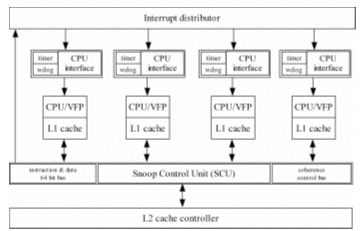
Fig 8 – ARM 11 MPcore
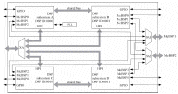
Fig 9 – Texas Instruments TMS320VC5441
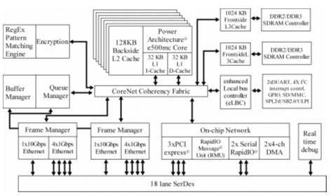
Fig 10 – QorIQ™ P4080
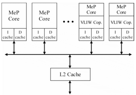
Fig 11 – Toshiba Venezia Architecture
Related Semiconductor IP
- ReRAM NVM in DB HiTek 130nm BCD
- UFS 5.0 Host Controller IP
- PDM Receiver/PDM-to-PCM Converter
- Voltage and Temperature Sensor with integrated ADC - GlobalFoundries® 22FDX®
- 8MHz / 40MHz Pierce Oscillator - X-FAB XT018-0.18µm
Related Articles
- Prototyping Mesh-of-Tree NOC Based MPSOC on Mesh-of-Tree FPGA Devices
- Control an FPGA bus without using the processor
- Pipeline Stage Resolved Timing Characterization of FPGA and ASIC Implementations of a RISC V Processor
- SoC Test and Verification -> Assertions speed processor core verification
Latest Articles
- An FPGA-Based SoC Architecture with a RISC-V Controller for Energy-Efficient Temporal-Coding Spiking Neural Networks
- Enabling RISC-V Vector Code Generation in MLIR through Custom xDSL Lowerings
- A Scalable Open-Source QEC System with Sub-Microsecond Decoding-Feedback Latency
- SNAP-V: A RISC-V SoC with Configurable Neuromorphic Acceleration for Small-Scale Spiking Neural Networks
- An FPGA Implementation of Displacement Vector Search for Intra Pattern Copy in JPEG XS