An HDTV SoC Based on a Mixed Circuit-Switched / NoC Interconnect Architecture (STBus/VSTNoC)
Abstract:
Even though nanometric CMOS technologies allow integrating several hardware resources into a single chip (SoC), a lot of difficulties arise for the on-chip interconnection. Classical physical issues such as congestion, frequency drop, parasitics effect are addressed in current literature by adopting NoC interconnect solutions.
This paper presents the interconnect solution adopted for an HDTV SoC developed in HVD division of STM. The SoC is a one-chip satellite HDTV set-top box IC developed in 65nm technology. The interconnect of this HDTV SoC is the first in STM implementing a mixed architecture based on the circuit-switched interconnect named STBus and the new NoC interconnect named VSTNoC.
This paper will highlight the studies and adopted solutions in terms of interconnect architecture and IP traffic generation to cope with the main requirements of this HDTV SoC:
- Reduce the integration complexity (wiring reduction, pipelined interconnect components)
- Cope with high bandwidth demanding
- Ensure a low latency for the CPU accesses to memory
The first section provides a short overview of the VSTNoC.
The second section provides an overview of the SoC interconnect.
The third section presents studies and justifications of the solutions adopted in this interconnect architecture. Two main subjects will be presented: interconnect partitioning and VSTNoC frequency sizing.
The fourth section provides achieved results and highlight benefits brought in by VSTNOC technology.
1.VSTNoC overview
The VSTNoC (Versatile STNoC), being still in circuit-switched category, is based on the current STBus approach and represents a first step towards a complete NoC solution.
VSTNoC stands for Versatile ST Network on Chip:
- Network on Chip comes from the packet format (header + payload) and the layered approach
- Versatile because it belongs to the topology dependent NoC family (VSTNoC topology depends on system topology).
The VSTNoC main benefit is the wire reduction, allowing reducing physical issues such as congestion, parasitic effects, frequency drop, mapping onto FPGA. Other benefits are area reduction and frequency increase.
Wire reduction comes from the header/payload multiplexing. The following table provides a comparison between STBus interfaces and VSTNoC interfaces:
| Interconnect | Interface wires |
| STBus type 3 (32 bits) | 178 |
| STBus type 3 (64 bits) | 245 |
| VSTNoC (36 bits flit) | 87 |
| VSTNoC (72 bits flit) | 157 |
Table 1: STBus and VSTNoC interface width
The flit stands for Flow Control Unit and represents the basic logic unit that can be transmitted over a logic link (channel) in a NoC. In case of VSTNoC the flit size is determined by the sum of data bus width (32 or 64 bit) and mask bus width (1 bit for each byte of data so 4 bit in case of 32 bit data bus, 8 bit in case of 64 bit).
The VSTNoC solution used in the SoC described in this paper is a 72 bits flit version.
The area reduction comes from wire reduction and removal of the dependencies between transmit and receiving paths, leading to smaller intermediate tracker buffers.
Frequency increase comes from the pipelined nodes architecture.
1.1 Traffic structure
VSTNoC arbitration granularity is the transaction. The transaction is the highest level transmission entity and it is a collection of packets.
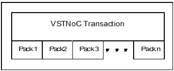
Fig 1: VSTNoC Transaction

Fig 2: VSTNoC packet
The packet is made of a header and a payload. The header brings the NoC routing information, the QoS information, the packet transfer size (4, 8, 16 or 32 bytes) and the type of transfer (read, write). The header requires 1 clock cycle to be transferred in a 72 bits flit VSTNoC and 2 clock cycles in case of 36 bits flit.
header transfer time = 1 clock cycle in 72 bits flit VSTNoC
header transfer time = 2 clock cycles in 36 bits flit VSTNoC
The number of clock cycles needed to transmit a packet depends on the flit size:
Packet_transfer_time = payload_transfer_time + header transfer_ time
where:
payload_transfer_time = packet_transfer_size (bytes) / data_bus_width (bytes)
As an example a 32 byte VSTNoC packet requires 5 cycles to be transferred (4 cycles for payload, 1 cycle for the header) in a 72 bits flit VSTNoC.
1.2 VSTNoC overhead
The usage of the VSTNoC technology leads to the introduction of the concept of overhead in the interconnect domain. The overhead is intrinsic in the NoC protocol because of the header/payload split, this leading to occupy the bus with non data information.
The VSTNoC requires one header for each packet. For VSTNoC transactions normally it is required one header for each packet of which the transaction is made of. In case of linear traffic (addresses of consecutive packets linearly incrementing) a unique header is required for the transaction, leading to minimize the overhead.
Considering the above points the overhead for a VSTNoC transaction will be given by the following formula:
Overhead = Number_Flit_of_headers_per_transaction / Number_Flit_of_payload_per transaction
As an example, assuming a linear traffic on a 72 bits flit VSTNoC, a transaction made of 8 packets each having a 32 byte transfer size, has the following overhead:
Overhead = 1/32 = 3.13%
If the transaction is made of a single packet having a 32 byte transfer size:
Overhead = 1/4 = 25%
This suggests that a correct sizing of VSTNoC transactions is fundamental to minimize the NoC overhead.
1. SoC Interconnect
The HDTV SoC on which the mixed interconnect has been implemented has to support multiple and concurrent internal processes. All these operations are based on memory to memory transfers; each block or system is responsible of specific data processing, but all data are stored in a shared DDR2 memory.
From a bus interconnect point of view this HDTV SoC can be seen as a group of IPs initiating traffic (we will call them Initiators in this paper) towards the memory systems (DDR2, Flash, other external peripherals) but also towards on chip configuration registers (we will call them targets). The HDTV SoC under presentation has the following characteristics:
| Description | Value |
| Die size | 64 mm2 |
| Gates count | 31 M |
| Number of STBus Initiators | 45 |
| Number of STBus Targets | 4 High bandwidth 60 Low bandwidth |
| DDR interface | 1 32 bits DDR2 interface or 2 16 bits DDR2 interfaces |
Table 1 : SoC main characteristics
The SoC interconnect (see figure 3) is built with local STBus-based clusters connected through a central VSTNoC node. Each cluster is constructed with a local STBus interconnect connecting either multiple initiators (initiator cluster) or multiple targets (target cluster).
Six STBus initiator clusters and four target clusters are implemented. Each cluster groups initiators or targets implementing one of the main SoC functions:
- Initiator clusters:
- Display cluster
- Composition cluster
- Transport cluster
- Video Decoder cluster
- Peripherals cluster
- Graphic cluster
- Target cluster:
- DDR IF0/IF1 clusters
- Flash/PCI cluster
- Register decoder cluster: this allows to access to all peripherals internal configuration registers.
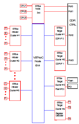
Fig 3: SoC interconnect
From a STBus point of view each STBus cluster (refer to figure 4 and 5) implements the following functionalities:
- STBus node arbitration among multiple initiators (in case of initiator cluster) or targets (target cluster). This function is implemented with the STBus node component.
- Size conversion to adapt initiators or targets STBus plug bus width to cluster node bus width but also to adapt cluster node bus width to that of the central VSTNoC node. This function is implemented in the STBus generic converter component and in the VSTNoC Network Interface .
- Frequency conversion to adapt cluster node frequency to central VSTNoC node interconnect. This function is implemented in the VSTNoC initiator network interface (INI) and target network interface (TNI) components.
- STBus to VSTNoC conversion to allow STBus transactions to be conveyed into VSTNoC channel. This function is implemented in the VSTNoC initiator network interface and target network interface components.
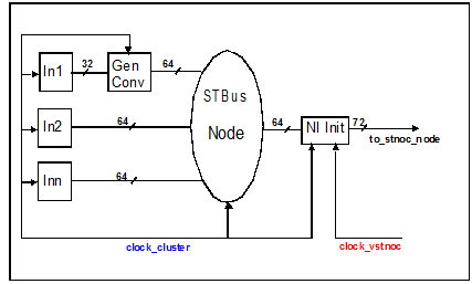
Fig 4: Initiator Cluster
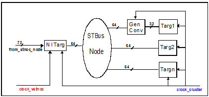
Fig 5: Target Cluster
The central interconnect is made of a 6x4 VSTNoC node and handles the communication between the initiator and target clusters. This is a full crossbar VSTNoC node that allows to manage concurrent traffics from multiple initiator clusters to multiple target clusters.
3. Definition of the interconnect architecture
The section presents studies and justifications of the solutions adopted in this interconnect architecture. Two areas have to be analyzed:
- Interconnect partitioning
- VSTNoC frequency sizing
The final interconnect topology is the result of studies aiming to address performances, physical and low power requirements.
The performances requirements drive mainly the clusters definition: each cluster groups IPs that have similar QoS (Quality of Service) requirements and most of the time contribute to implement a specific SoC function (i.e. transport, display, etc..). As an example the IPs grouped in the Display cluster have real time constraints while the Graphic accelerator cluster does not (graphic planes can be composed in advance to their presentation by using a memory to memory approach, allowing to treat this as non real time process) . The arbitration scheme used in the central 6x4 VSTNoC node uses a priority based algorithm. The priority level associated to each of its six initiator ports is programmable. Each of these six initiator ports is connected to a STBus initiator cluster. This allows to assign the same QoS to IPs grouped in the same cluster.
A special cluster is the one dedicated for CPUs. CPU performance requirements imply to minimize the latency to access the DDR. To achieve this, the CPUs traffic do not cross the central VSTNoC node and use a dedicate STBus channel to access the DDR controller (refer to figure 3). The DDR controller has a dedicated STBus target for connection with this channel.
The cluster definition has to take into account also the SoC floorplan constraints.
The SoC top-level is constructed with three physical partitions (refer to figure 7), the size of each is manageable by Back-End tools.
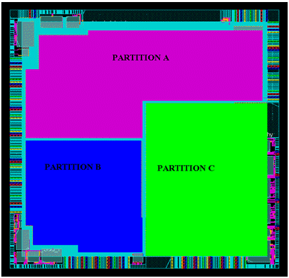
Fig 7: SoC Top Level partitioning
Each physical partition contains one or multiple STBus clusters (refer to figure 8)
The following two main rules have been followed:
- IPs that are part of the same cluster must be placed in the same physical partition to avoid to use STBus links at top-level so to reduce top level wiring
- Inter-partitions communication has to be performed using VSTNoC links since this will ensure the minimum top level wiring. The central VSTNoC node has to be placed inside the partition containing the majority of the initiator and target clusters as long as the size of this partition is still acceptable
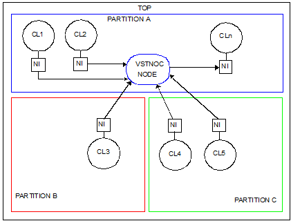
Fig 8: Clusters mapping inside partitions
The usage of the central VSTNOC node allows to minimize the top level wiring. The VSTNoC node is placed in one of the three partitions and each cluster communicates with it through its dedicated Network Interface.
The cluster definition is also driven by low power requirements: grouping of certain IPs inside the same cluster aims to facilitate the clocking management (clock stop and clock frequency reduction).
As an example: in applications where neither USB nor Ethernet interfaces are required the Peripheral cluster clock can be switched off.
In applications where the graphic accelerator is not required, the graphic cluster can be switched off.
In power saving mode the transport cluster clock can be switched off or its frequency may be slowed-down.
3.2 VSTNoC frequency sizing
To compensate the overhead introduced by VSTNoC, its clock frequency has to be sized correctly to ensure that the interconnect does not impact the DDR efficiency. In fact, since the traffic from all system initiators will cross the central VSTNoC, it has to be ensured that the DDR controller is fed efficiently by the VSTNoC node in the transmit path (commands and write data) and, at the same time, the DDR controller has to not be stalled by VSTNoC when providing the response read flow to the system (refer to figure 9)

Fig 9: TX/RX flow VSTNoC/DDR controller
An analytical model calculating both DDR and VSTNoC overheads is used to determine the minimum VSTNoC frequency in order to not impact the required average throughput required on DDR2. The following steps have been followed:
1- Identify the worst case application scenario
2- Calculate the total bandwidth (MB/sec) required on DDR2 interface to support the scenario identified. Both TX flow (commands and write data) and RX flow (read data) have to be considered. Let’s call these two as bw_in_tx and bw_in_rx.
3- Describe VSTNoC traffic initiated by each IP process involved in the scenario. That implies to describe each process in terms of: a) required throughput (MB/sec) b) VSTNoC traffic shape that is the size in byte of the transaction used.
4- Calculate VSTNoC overhead (in % )
5- Calculate frequency (MHz) needed to evacuate the overall VSTNoC traffic that is made of header and payload. This provides the average frequency figure needed to evacuate the overall traffic across the VSTNoC. For the two TX and RX flows this will be given by:

Fig 10: VSTNoC bandwidth
bw_out_tx and bw_out_rx is the bandwidth of the overall traffic (refer to figure 10) crossing the VSTNoC made of payload and header and is function of the overhead calcuted in step2:
bw_ou_rx= (1+overhe ad_rx)* bw_in_rx
6. If the resulting frequency from point 5 is smaller than that of the DDR controller (400 MHz) the average and peak DDR efficiency have to be taken into account to ensure the VSTNoC node is able to absorb the traffic at this higher rate.
7. Calculate the average DDR efficiency (in %). This is calculated in a video frame period. Knowing the traffic shape of each process feeding the DDR controller, it is possible to calculate the number of DDR cycles it will take in terms of memory access: the total number is given by the sum of DDR cycles consumed to transfer the full burst plus the cycles consumed to execute DDR protocol commands (precharge, activate, etc). A statistical approach is used to determine the distribution of bursts among the four or eight banks of which a DDR device is built of. If ddr_aveg_eff is the calculated DDR efficiency, the VSTNoC should be clocked at least with a minimum frequency equal to:
VSTnoC_Min_Freq_Awg = DDR_freq*ddr_aveg_eff.
8. Calculate the peak DDR efficiency. This is calculated in a smaller timing window where two optimistic conditions can be applied: a) only read traffic crossing the interconnect (this leads to not pay the bus turn-around overhead). b) No traffic provoking the worst DDR overhead (page miss over the same DDR bank). This two conditions lead to optimize the DDR efficiency. The VSTNoC has to be able to absorb these peaks avoiding so to stall the DDR controller. This leads to estimate the VSTNoC frequency as:
VSTnoC_Min_Freq_Peak = DDR_freq*ddr_peak_eff.
9. The DDR controller (in very short timing windows) can provide read response traffic at full DDR frequency (400 MHz). This is the case of page hit traffic, in particular three read bursts, each of 256 bytes, sent in the same DDR page have been taken into account. To absorb efficiently these short peaks, the fifos in the Network interface connected to the DDR controller have been sized accordingly.
Applying the above steps to the design under study, the following results have been obtained:
Step 1: As an example the following scenario has been used:
- 1 HD H264 decode
- 1080i on primary HD display
- 3 Graphic HD (1920*1080) planes 16 bpp on primary HD display
- 480i on secondary SD display for resized content of HD display (video and graphic planes)
- Two transport inputs at 80Mb/sec for record to HDD and time shift playback
- Streaming out on Ethernet MII interface at 100 Mb/sec
Step 2
: The scenario requires 700 MB/sec for TX flow and 1400 MB/sec on read flow.
Step 3 to 5: The VSTNoC required frequency to evacuate the overall traffic (payload plus header) is 183 MHz, being calculated considering the RX flow.
Step 6: The conditions to move to step 7 are met.
Step 7: 8: Over a short timing window the peak DDR efficiency is 70% so:
VSTnoC_Min_Freq_Peak = 280 MHz
This has been rounded to 300 MHz.
Step 9: An appropriate sizing of the fifos of the target network interface target connected to the DDR controller has been done to absorb DDR peaks on response read traffic.
4. Conclusions
This first SoC developed using a mixed STBus/VSTNoC interconnect solution can be considered a good test case to explore some of the VSTNoC benefits and highlight aspects to improve.
The usage of the VSTNoC solution has allowed a fast timing convergence. This is due to the deeper pipeline implemented in the VSTNoC components. This extra pipeline anyway does not represent an additional area to pay since the extra stages of pipeline have been treated as part of the overall interconnect fifos sizing. In this SoC the overall interconnect represents the 3% of the SoC core area.
It has also been proven the expected increased scalability. The central 6x4 VSTNoC targeting 300 MHz has been finally implemented successfully at 400 MHz to bring extra margin.
It has been proven also that the embedded VSTNoC overhead is negligible compared to typical DDR efficiency as long as IPs traffic is well sized in terms of transactions size.
The usage of the Network Interface component has allowed to easily connect STBus clusters to central VSTNoC. Conveying STBus traffic in the VSTNoC link is almost transparent and the only precaution to take is to guarantee an efficient size of the STBus bursts that the NI maps on VSTNoC transactions.
The definition of the VSTNoC packet allows also to easily integrate IPs not initiating STBus traffic (AXI, OCP, etc.). The INI and TNI implements the IP to VSTNoC traffic conversion.
The wiring reduction helped in reducing the integration complexity. The benefit would have been even higher in case of a more complex SoC topology (i.e. SoC using a higher number of high bandwidth internal targets).
The inter-partitions communication could be improved to avoid the synchronous communication between partitions (link NI-VSTNoC node) in the high speed VSTNoC clock domain.
Thanks to STM OCCS team providing the VSTNoC/STBus technology.
Related Semiconductor IP
- NPU IP Core for Mobile
- NPU IP Core for Edge
- Specialized Video Processing NPU IP
- HYPERBUS™ Memory Controller
- AV1 Video Encoder IP
Related White Papers
- Performance Verification Methods Developed for an HDTV SoC Integrating a Mixed Circuit-Switched / NoC Interconnect (STBus/VSTNoC)
- A Multi-Objective Optimization Model for Energy and Performance Aware Synthesis of NoC Architecture
- A Multiprocessor System-on-chip Architecture with Enhanced Compiler Support and Efficient Interconnect
- 3D IC 2-tier 16PE Multiprocessor with 3D NoC Architecture Based on Tezzaron Technology
Latest White Papers
- Ramping Up Open-Source RISC-V Cores: Assessing the Energy Efficiency of Superscalar, Out-of-Order Execution
- Transition Fixes in 3nm Multi-Voltage SoC Design
- CXL Topology-Aware and Expander-Driven Prefetching: Unlocking SSD Performance
- Breaking the Memory Bandwidth Boundary. GDDR7 IP Design Challenges & Solutions
- Automating NoC Design to Tackle Rising SoC Complexity