A Multiprocessor System-on-chip Architecture with Enhanced Compiler Support and Efficient Interconnect
Department of Communications and Integrated Systems, Tokyo Institute of Technology
2-12-1 Ookayama, Meguro-ku, Tokyo, 152-8550, Japan
ABSTRACT
This paper describes the development of a Multiprocessor System-on-Chip (MPSoC) with a novel interconnect architecture and an enhanced compiler support for programmability. Our MPSoC programming framework - which we call Tightly-Coupled Thread (TCT) model - is aimed in significantly simplifying the task of system-level partitioning and concurrent behavioral modeling. A designer only needs to use a simple syntax on the sequential program to specify the program partitioning, and by using a powerful TCT compiler, the interprocessor communication operations are automatically generated. Our MPSoC architecture is based on an existing AMBA-based SoC platform with a predesigned RISC core acting as the host CPU and a multiprocessor-array block with 6 processing elements as a slave device. Our interconnect architecture and a dedicated hardware communication module IP embedded in each processing elements and in the host CPU interface allows a seamless integration to implement a heterogeneous MPSoC.
1. INTRODUCTION
We are developing a new framework for Multiprocessor Systemon- chip (MPSoC) [3] design which we call Tightly-Coupled Thread (TCT) model. The main aim of the TCT model approach is to simplify the programming model for MPSoCs designs. Compared to the existing approaches used for the programming of MPSoC [4]- [9], the TCT model offers the following advantages:
- The TCT model allows the specification of system partitioning directly on a reference C code. Thus very early in the design stage, system partitioning and performance estimation analysis can be performed. This will help the designer to quickly achieve the desired performance for the MPSoC implementation.
Other than that, because the partitioning is done at C-code level, the TCT Model is mainly platform independent. Both homogeneous and heterogeneous multi processor systems can be targeted by the TCT model.
- The TCT compiler handles automatic insertion of interprocessor communications and automatically generates the concurrent execution model. This frees the designer from dealing with time-consuming and error-prone task of modeling the interactions between concurrent processes.
- A complete data dependency analysis that covers the whole program guarantees the correctness of parallel execution model based on the correctness of sequential execution model. This will greatly reduced the effort needed for debugging process.
The focus of this paper is to describe the development of an MPSoC architecture that will be used as a proof-of-concept vehicle for validating the feasibility of our TCT model approach. This paper is organized as follows. Section 2 introduces the basic of TCT model. Section 3 discusses the overall MPSoC architecture. The communication infrastructure and interconnect are described in Section 4. Section 5 presents the experimental results and some discussions. The detail of LSI implementation of the MPSoC is presented in Section 6. The paper is summarized in Section 7.
2. TIGHTLY-COUPLED THREAD MODEL
It is a common practice to start modeling the behavior of a system using sequential programs such as C language. The TCT programming model allows the partition of a sequential program written in C into concurrent processes. In the TCT model, the only task for a designer is to insert a set of thread scopes on the original sequential program. A thread scope indicates a separate concurrent process, which we simply refer to as threads, to be executed on a (separate) processing element.
Thread scope statement: Syntax is given as:
THREAD(name){ statements }
The part “THREAD(name)” is called the thread scope header, and the following “{ statements }” is called the thread scope. Basically any compound statement in C is allowed in the thread scope. For current compiler implementation, some exceptions exist. Those are goto statement, dynamic memory allocation statements (malloc, free), pointers to pointers (only single-level pointers supported), and pointers to functions. These exceptions exist only because their practical implementation brings unnecessary complexity, and not due to the limitation of the TCT programming model itself. Other than that, equivalent functionality can be achieved using different approaches. However, the omission of some of these restrictions is planned for future versions of the compiler.
Compatibility to C: By inserting a preprocessor which simply erases the thread scope header (such as #define THREAD(n)), computationally equivalent executable can be generated by a standard C compiler.
An example of the use of TCT model on a real world application is shown in Figure 1. Figure 1 shows an example of a parallel Ccode for JPEG encoder (modified from the original source [2]) modeled in TCT.
In function JPEGtop, there are five thread scopes inserted in the code: Dsamp, BLKcore, Y0, Y1, and C. The function ReadOneLine, which is called by the JPEGtop function, has four threads, three of them cY, cCb, and cCr are for the reading of each image component. The core function BLK8x8 – which contains three threads Q, E, and W – are called by three threads: Y0, Y1, and C. Furthermore, the function BLK8x8 also calls the DCTCore function which contains two threads scopes Dr and Dc.
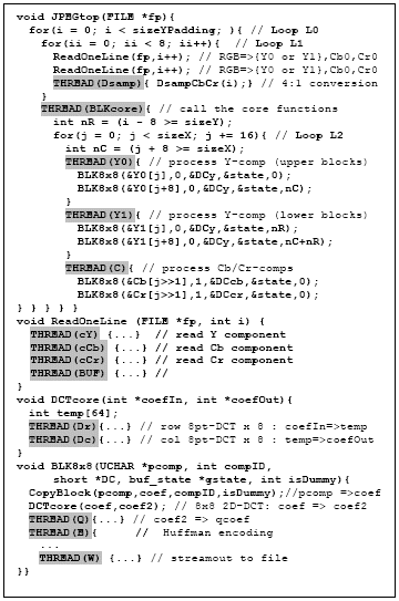
Figure 1. JPEG encoder with thread scopes
The major source of parallelism in the TCT model is obtained from a combination of functional pipelining and task parallelism applied to loop structures and functions. For the JPEG encoder thread-slicing structure shown in Figure 1, its parallel processing scheme is depicted in Figure 2.
-
In loop L0, inner loops L1 (root-thread) and L2 (thread BLKcore) form a 2-stage pipeline.
-
In loop L1, calls to ReadOneLine (root-thread) and DsampCbCr (thread Dsamp) form a 2-stage pipeline.
-
Inside the function ReadOneLine, task parallelism is applied using threads cY, cCb, and cCr. Combined with the BUF thread, a 2-stage pipeline is formed.
-
Inside the function BLK8x8, its base-thread and the five threads Dc, Dr, Q, E, and W form a 6-stage pipeline.
-
Task parallelism is applied to loop L2 where the six calls to BLK8x8 are invoked from three threads Y0, Y1, and C in which three sets of the above 6-stage pipeline execute in parallel (these three pipelines are not independent since there are data dependences between these pipelines).
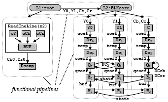
Figure 2. Pipelines and parallelism in JPEG encoder
Some major properties of the TCT model are as follows.
-
Thread scopes can encompass large variation of computation granularities (statements, loops, functions) and can also have hierarchical structures.
-
Each thread is executed by program-driven (statically scheduled) process.
-
Thread synchronizations, on the other hand, are implemented by data-driven message-passing model (similar to data-flow machines) to realize a complex pipelined network.
-
Thread synchronizations operations are automatically generated by the TCT compiler based on interprocedural data dependency analysis to guarantee computational equivalency to its sequential execution model.
-
The TCT compiler currently supports only 1 thread per Processing Element (PE). This limitation is planned to be omitted in the next version of the compiler by using multi threading techniques to support multiple threads per PE.
-
Currently the TCT is targeted for distributed-memory architectures (without any shared memory) only. Extension to support distributed-shared memory system is planned.
3. TCT MPSoC ARCHITECTURE
To validate the feasibility of our TCT model approach, an MPSoC architecture that will be used as a test vehicle has been designed. Its block diagram is shown in Figure 3.
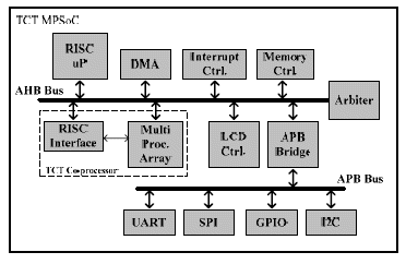
Figure 3. TCT MPSoC
The designed MPSoC is based on an existing AMBA-based [1] SoC platform. The AHB bus is clocked at 100MHz, while the APB bus is clocked at 50MHz. The SoC consists of a 32-bit RISC processor and various general input-output IPs such as serial and parallel port, and also an LCD controller. A TCT Co-processor block is then added to the AHB bus. This block is used as the main engine to run applications modeled using TCT.
A detailed block diagram of the TCT Co-processor is shown in Figure 4. The TCT Co-processor basically consists of a multiprocessor-array and a RISC-interface. The TCT Coprocessor has 2 connections to the AHB Bus. One is to the RISCinterface; the other is to the Memory Control Block (MCB) controller of the multiprocessor-array.
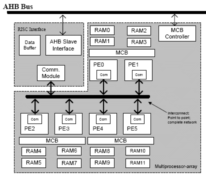
Figure 4. TCT Co-Processor
The multiprocessor-array is built with 6 Processing Elements (PE). The decision to use 6 PEs is constrained by the availability of silicon area. The PE is a custom-built 4-stage pipelined 32-bit RISC. Each PE is equipped with a communication module used for data transmit and receive operation with the other PEs.
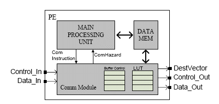
Figure 5. Communication Module within PE
A simplified block diagram of the communication module is shown in Figure 5. The communication module is integrated into the processor’s pipeline stage as a multi-cycle operation module. It generates a communication hazard to stall the pipeline when a data-sync hazard or data-transfer hazard occurs. To reduce communication setup time, the communication module uses a lookup table (LUT) that contains information necessary for data transfer operations, such as data store address and data transfer size. The content of LUT is automatically generated by the TCT compiler.
There are 12 blocks of 4 Kbyte RAM in the multiprocessor-array. The Memory Control Block (MCB) is used to configure the allocation of memory to each PE. In the simplest configuration, each PE is allocated with 4 Kbyte of Program Memory and 4 Kbyte of Data Memory. Additionally, also through the MCB, every RAM blocks can be addressed from the AHB Bus. This is useful for the initialization of program and data memory for each PE.
The RISC-interface is used to allow the RISC to act as the 7th PE of the multiprocessor-array. It employs the same communication module used for the PE. The difference is that instead of working with data memory; it uses the available 2*4 Kbyte data buffers. Moreover, the RISC processor is able to continue the program execution while the RISC-interface is communicating with the other PE (contrast to the communication module within PE which is integrated into the processor’s pipeline).
When the RISC processor needs to transfer data to another PE, first it checks the status of the RISC-interface. If the RISCinterface is idle, the data to be transferred is then written to the RISC-interface’s buffer. Once the data transfer finishes, the RISC processor is able to continue the program execution. The actual data transfer operation to the eventual destination PE, including communication setup, is then handled autonomously by the RISCinterface.
For the reverse data communication from a PE to the RISC processor, the PE ordinarily communicates with the RISCinterface. The transferred data is written to the RISC-interface’s buffer. Once the data transfer is completed, the RISC-interface generates a data-receive interrupt to the RISC processor. The interrupt handler of the RISC processor then reads the data from the RISC-interface’s buffer.
The implementation of the RISC-interface is an actual example of embedding the communication module into an existing off-theshelf processor. The integrated processors can then be used as one of the processing elements within the multiprocessor architecture. The same mechanism using the same communication module can also be applied to various types of hardware-IPs, opening up large possibilities for various types of MPSoC architectures where TCT model can be implemented.
4. MPSoC INTERCONNECT
The PEs (and also including the RISC-interface) are connected to each other through a point-to-point complete interconnect network. The interconnect network used in the multiprocessor array is a full crossbar architecture with autonomous arbitration mechanism for simultaneous requests to same destination (nonblocking data transfer). The autonomous arbitration is realized by the use of simple n:1 MUXes where n = number of PEs + 1 (the plus one is for the RISC-interface). The n:1 MUX architecture is realized with a binary MUX tree. Each MUX has a priority bit register to select one out of two sources in case of simultaneous requests. These priority flag registers are directly controlled by a dedicated instruction at each processing element. The overall interconnect network is shown in Figure 6. The block diagram of the MUX and 7:1 MUX is shown in Figure 7. This autonomous arbitration scheme uses a high-speed and area-efficient circuit. The interconnect latency is 2 ns and the gate count is roughly 1K.
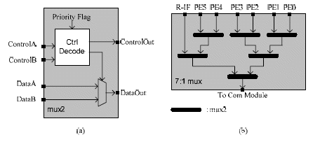
Figure 7. (a) MUX (b) 7:1 mux
4.1 Communication Port
The output port of each communication module consists of a (2+2) bits of control, a 32-bit data and an n-bit destination vector. Two separate control lines for transmit request and receive response, each 2-bit wide, is used to transmit the active communication protocol. The possible transmit request protocol are: ‘NULL’, ‘REQ’, and ‘TRANS’, while the possible receive response protocol are: ‘NULL’, ‘ACK’, ‘LATEACK’, and ‘NACK’. The ACK response from the receiver indicates “bus grant” for the corresponding transmitter. Furthermore, the data transmission path, once established with REQ->ACK sequence, is protected by unconditionally selecting TRANS signal (indicating that data transmission is in progress) over REQ at the MUXes.
Input port, on the other hand consists of (2+2)-bit control and 32- bit data which are autonomously arbitrated by the MUX tree as described above.
The destination vector is used by the n:1 MUX module to check whether the incoming signals are intended for the corresponding receiver or not. If it is not, the incoming signals are masked.
4.2 Buffered Communication Channel
Data transfer operations between processor pairs are maintained by assigning logical port-IDs at the receiver processor, which is transferred on the data lines during REQ phase and is used to access the communication LUT at the receiver for address generation. Each logical port can be individually buffered or unbuffered, depending on the application and the available memory size.
Individually buffered ports are further divided into 2 buffer types to handle different buffer depths requirements. Depths of these 2 buffer types are programmable at compile time within the range of 0 to 63. Up to 256 logical port-IDs are supported, and individual buffer management is implemented inside our communication module.
4.3 Communication Protocol
The communication protocol employed in current MPSoC is based on a simple hand-shake protocol. The communication protocol can be divided into the following phase.
-
Setup: Asserts destination port-ID on data bus and simultaneously asserts a REQ signal on control bus.
-
Response: Checks buffer status on requested port-ID and respond with ACK (granted) or NACK (rejected due to buffer full). Data transfer size and store address are then retrieved from the communication LUT indexed by port-ID.
-
Transmit: Upon receiving back an ACK, asserts TRANS signal on control bus, and simultaneously load the transmitted data to the data bus. The transmit operation supports data-burst transfer, one word per cycle.
-
Transmit retry: When responded back by a NACK, the transmitter waits for a LATEACK from the receiver (i.e. buffer is now available), then restarts the setup phase. The use of LUT within the communication module improves the setup time because then it is only the portID that needs to be transferred from the source to the destination. For further improvement, some LUT caches strategy are employed within the communication module. The communication setup time thus ranges from 2 to 6 cycles (typical is 4 cycles for single-word transfer).
5. EXPERIMENTAL RESULTS
For the purpose of preliminary evaluation to the performance of the designed MPSoC, the parallelized JPEG program is compiled, and then the generated instruction opcodes are simulated using the TCT simulator, which was built into the TCT Compiler.
Because multithreading support has not been implemented in current MPSoC, the number of thread is limited to the number of available PEs. Thus, the JPEG program to be used for the experiment is parallelized into five threads. The thread scopes used are (also refer to Figure 1): root, BLKCore, Q, E, and a new thread DCT that encapsulate the whole DCTCore function.
Using this thread slicing strategy, basically a 5-stage pipeline is formed. The first pipeline stage (thread: root) calls the function ReadOneLine twice, and then continues with the downsampling operation. The second pipeline stage (thread: BLKCore) executes Loop 2 and making 6 calls to core function BLK8x8 (the function calls are executed sequentially). The function BLK8x8 itself is implemented as a 3-stage pipeline process using threads DCT, Q, and E.
The experimental results are presented in Table 1. The cycle run time is obtained from the TCT simulator. The TCT simulator runs at instruction level, and also able to model various types of hazards and communication protocol fairly precisely. For example, using the Verilog RTL implementation of TCT MPSoC, the simulation of JPEG Encoder program with 5 threads took 4,039,924 cycles to complete, while the TCT simulator took 4,038,888 cycles. It means in 4M cycle of program execution, the differences are only about 1,000 cycles.
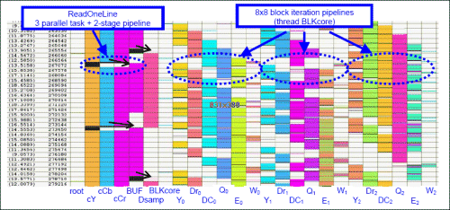 Figure 8. Execution trace for thread slicing of Figure 1
The top half of the table shows the simulation result for running a JPEG encoder program with five threads using a 128 pixel by 149 pixel image as the input. Compared with the time needed to complete a pure sequential program (the number of thread is one, and no communication-related instructions are inserted), the simulation shows an overall performance speedup of almost 3.0. With 5 processing elements, this yields about 60% parallel efficiency.
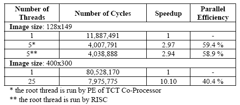
Table 1. JPEG Encoder Execution Time
The execution of root thread is done in two ways, by using the PE inside the TCT Co-processor block and by using the RISC processor. For the second case the observed number of cycles is slightly increased. The probable cause is the additional time needed for communication between the RISC processor and the RISC-interface. The communication scheme using buffer memory inside the RISC-interface implies that ‘double’ data transfer operations are needed (from RISC’s data memory to RISCinterface’s buffer and then to PE, and vice versa). Even though with this scheme the processor execution and data transmission can run concurrently, the time needed for data transfer outweigh this advantage. However, the experimental result clearly shows that the RISC-interface does not impose a considerable penalty and is able to work as efficiently as the communication module used within PE.
The bottom half of Table 1 shows the results for running the JPEG encoder program with a more aggressive thread slicing strategy, in which the program is divided into 25 threads. The details of thread slicing strategy are already presented in Section 2. Employing this strategy, the TCT simulator shows a speedup of 10.10 and parallel efficiency of 40.4% is achieved.
Using the scheduler tool built into the TCT compiler, a program execution trace can also be obtained. A snapshot is presented in Figure 8. The left part of execution trace shows the parallel execution of ReadOneLine function: three parallel tasks of cY, cCb, and cCr, and then pipelined with BUF thread. The Dsamp thread is executed after every two thread-cycle executions of BUF thread. In the right part, three parallel executions of BLK8x8 function are shown; each consists of a 6-stage pipeline process.
A further analysis to the execution trace reveals that the major bottleneck of current pipelining scheme is in Loop 1 of JPEGtop function (the left part of execution trace). Large loops within the threads inside this loop create unbalanced pipeline stages for the overall program execution, especially in relation with the BLKCore thread shown on the right part. Balancing the pipeline stages will improve the overall performance. This could be achieved for example by parallelizing the large loops even further, using various available techniques for loop transformation. A more advanced approach by implementing a dedicated hardware to optimize the execution time of for long pipeline stages is another option.
6. TCT MPSoC LSI IMPLEMENTATION
The MPSoC is synthesized using the TSMC 0.18u library. The area utilization is presented in Table 2.
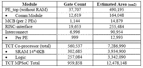
Table 2. LSI Area Utilization
The gate count for interconnect per PE is roughly 1K gate which is negligible compared to the PE itself. Rather, the interconnect area is wire-dominated (number of horizontal wires in Figure 6). Based on preliminary floor planning, the interconnect layout height is estimated at 167 um and the total interconnect area is 472,944 um2 (the width of multiprocessor-array is estimated at 2,832 um).
The communication module occupies about one-third of PE area. This is roughly equivalent to the 32 * 32-bit register file used inside the PE.
The first sample of the chip is scheduled to arrive at the end of this year. The first plan is to run H.264 video decoding application modeled in TCT using this chip.
7. SUMMARY
The TCT MPSoC described in this paper uses a generic and high portable interface for the integration of multiprocessor and hardware-IPs. The communication module embedded within the multiprocessor array can be easily used for other off-the-shelf processors and even hardware IPs, such as shown within the RISC interface where a communication module is effectively attached to the AHB system.
Our full crossbar architecture with autonomous arbitration serves as a generic SoC interconnect platform for generating optimized application-specific interconnect architectures that require less connectivity than a full crossbar. Nevertheless, changes in interconnect topology has minimal effect on the implementation of the communication module.
The experience we obtained in the course of designing the MPSoC described in this paper gives us a higher confidence level to the versatility of TCT model approach. It is proven that existing IPs can be integrated as one of the processing elements for the concurrent execution of applications modeled in TCT. This shows large opportunities where the TCT programming model can be implemented on various types of MPSoC platform.
8. REFERENCES
[1] ARM Holdings PLC, “Advanced Microcontroller Bus Architecture (AMBA) specification rev 2.0”, 2001.
[2] Independent JPEG Group, http://www.ijg.org/
[3] Jeraya, A.A., Tenhunnen, H., and Wolf, W., “Multiprocessor System-On-Chips”, IEEE Computers, vol. 38, pp. 36-40, 2005.
[4] de Kock, E.A., “Multiprocessor Mapping of Process Networks: A JPEG Decoding Case Study”, in Proc. International Symposium on Systems Synthesis (ISSS), pp. 68-73, 2002.
[5] Youssef, M.W., Yoo, S., Sasongko, A., Paviot, Y., and Jerraya, A.A., “Debugging HW/SW Interface for MPSoC: Video Encoder System Design Case Study”, in Proc. 41st Design Automation Conference, pp. 908-913, 2004.
[6] OpenMP, http://www.openmp.org
[7] The Message Passing Interface (MPI) Standard, http://www-unix.mcs.anl.gov/mpi/
[8] Paulin, P.G., Pilikington, C., Langevin, M., Bensoudane, E., and Nicolescu, G., “Parallel Programming Models for a Multi-Processor SoC Platform Applied to High-Speed Traffic Management”, in Proc. International Conference on Hardware Software Codesign, pp. 48 – 53, 2004.
[9] Pazos, N., Ienne, P., Leblebici, Y., and Maxiaguine, A., “Parallel Modelling Paradigm in Multimedia Applications: Mapping and Scheduling onto a Multi-Processor System-on-Chip Platform”, Int. Global Signal Processing Conf., 2004.
Related Semiconductor IP
- 8MHz / 40MHz Pierce Oscillator - X-FAB XT018-0.18µm
- UCIe RX Interface
- Very Low Latency BCH Codec
- 5G-NTN Modem IP for Satellite User Terminals
- 400G UDP/IP Hardware Protocol Stack
Related Articles
- Interstellar: Fully Partitioned and Efficient Security Monitoring Hardware Near a Processor Core for Protecting Systems against Attacks on Privileged Software
- An Open-Source Approach to Developing a RISC-V Chip with XiangShan and Mulan PSL v2
- A 16 nm 1.60TOPS/W High Utilization DNN Accelerator with 3D Spatial Data Reuse and Efficient Shared Memory Access
- An HDTV SoC Based on a Mixed Circuit-Switched / NoC Interconnect Architecture (STBus/VSTNoC)
Latest Articles
- SNAP-V: A RISC-V SoC with Configurable Neuromorphic Acceleration for Small-Scale Spiking Neural Networks
- An FPGA Implementation of Displacement Vector Search for Intra Pattern Copy in JPEG XS
- A Persistent-State Dataflow Accelerator for Memory-Bound Linear Attention Decode on FPGA
- VMXDOTP: A RISC-V Vector ISA Extension for Efficient Microscaling (MX) Format Acceleration
- PDF: PUF-based DNN Fingerprinting for Knowledge Distillation Traceability