Performance Verification Methods Developed for an HDTV SoC Integrating a Mixed Circuit-Switched / NoC Interconnect (STBus/VSTNoC)
Grenoble France
Abstract:
As modern SoC integrates more and more IPs sharing the same external memory resource, it is essential to verify in the early stages of the SoC specifications and design that the on-chip bus and memory controller are optimized to deliver the performance required by the targeted application (memory bandwidth, latency, …)
This paper presents the performance verification methods that were set up and used for a SoC recently developed at STM. The SoC is a one-chip satellite HDTV set-top-box decoder IC. It integrates many memory-bandwidth demanding IPs sharing one or two DDR2 memories. The SoC interconnect uses two bus protocols: a circuit-switched interconnect named STBus and the new NoC interconnect named VSTNoC.
The SoC performance verification uses an incremental approach. First, an analytical and statistical method provides early performance figures of the SoC. As the design progress, a simulation platform using cycle-accurate models of the interconnect and memory controller is used to verify the application and produce more accurate performance figures. These results are important to confirm or refine the SoC architecture.
The results of these verification methods are presented and compared, as well as their correlation with silicon performance measurements.
Performance verification methods developed for an HDTV SoC integrating a mixed circuit-switched / NoC interconnect (STBus/VSTNoC)
I – HDTV SoC Overview
1 - SoC description
The SoC presented in this paper is a one-chip satellite HDTV set-top-box decoder IC. It integrates many memory-bandwidth consuming IPs sharing a one or two DDR2 memories. A mixed circuit-switched/NoC interconnect was designed to handle the communication of about 45 traffic initiators towards 60 targets. The initiators include 3 CPUs, Video and the Graphics processors, standard interfaces (Ethernet, SATA, USB…), transport processors and DMA engines. Among the 60 targets, there are 4 high-bandwidth demanding targets. A typical application exchanges near 2 GBytes/s of data over a 32-bits DDR2 memory bus clocked at 400MHz.
2 – Mixed circuit-switched / NoC interconnect
The interconnect connects IPs having different constraints:
- CPUs: their performances are sensitive to the memory access latency, especially in case of cache miss.
- Real Time IPs: their request to memory must be served in time to avoid breaking their functioning.
- Other IPs: they work with relaxed constraints regarding their access to the memory.
In the interconnect topology, the IPs are grouped in STBus clusters (circuit-switched bus) taking into account their traffic constraints, frequency, bus width and type.
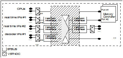
Fig.1: Mixed STBus/VSTNoc interconnect
All the traffics from the STBus clusters converge toward a central node. To achieve a high frequency, a NoC technology was selected to implement this central module. Initiators Network Interfaces (INI) convert STBus traffic coming from the different IP clusters into VSTNoC traffic. Target Network Interfaces (TNI) do the reverse conversion.
Regarding this mixed interconnect architecture, two important design points impacting the SoC performance must be particularly considered:
- The specification of the VSTNoC node clock frequency
- The sizing of the Network Interfaces (INI and TNI)
Compared to circuit-switched bus (STBus) the NoC technology (VSTNoC) uses more cycles to transfer the same amount of data (due to header/payload structure).
Examples of VSTNoC bus cycles overhead compared to STBus are given in the following waveforms. Figure 2 describes the request path and figure 3 describes the response path.
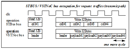
Fig.2: STBus versus VSTNoC bus cycles usage (request path)
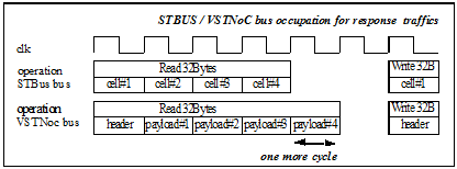
Fig.3: STBus versus VSTNoC bus cycles usage (response path)
To define the minimum VSTNoC frequency, the global NoC overhead must be computed for the application under analysis. The method consists in computing the bus cycle overhead (in percentage) for each IP traffic.

This percentage is multiplied by the memory bandwidth (in MBytes/s) requested by the IP in the application. This provides the equivalent STBus bandwidth in VSTNoC. All the IP bandwidths are added. Finally, the total bandwidth (MBytes/s) is translated in MHz considering the STBus/VSTNoC data bus width:

This analysis was conducted in both paths (transmit and response paths) to determine the minimum frequency to achieve the application required performance.
So, the minimum VSTNoC frequency has been carefully chosen to avoid any performance drop when the traffics cross the VSTNoC interconnect.
2.2 STBus/VSTNoC interface sizing
Another key point of the interconnect performance is to get a traffic as compact as possible at the memory interface to optimize the memory accesses. Otherwise, there could be a SoC performance drop due to an under-utilization of the shared memory resource. Potentially, each conversion in the interconnect can introduce bubbles in the traffic.

Fig.4: STBus/VSTNoC conversion
In the above figure, an IP sends a STBus transaction with a clock CLK1 to the VSTNoC node clocked with clock CLK2. If the data buses have the same size but if the frequency of CLK1 is less than the frequency of CLK2, then there is a risk to create bubbles inside the VSTNoC transaction. A store & forward mechanism can be used in the converter to accumulate locally in a FIFO, the x first cells of the burst before beginning the transmission on the VSTNoC side. The FIFO depth depends on the CLK1/CLK2 ratio, the bus widths and the traffic shape.
On the response path, the FIFO is sized in order to accept all the responses coming back to a lower frequency clock domain. An undersized FIFO can stall the memory controller and prevents new transactions to be sent to the DDR.
II - Performance verification context
The SoC performance verification context is strongly influenced or driven by the following three topics:
- Application: The performance verification is done for a defined application. Its characterization is detailed in the first paragraph of this section.
- IP traffic shape: The SoC uses IPs which have traffic characteristics. This point is presented in the second paragraph.
- DRAM timings: Unlike SRAM, DRAM accesses have more or less timing overhead. The third paragraph highlights this point.
First, the application is analyzed and broken down into IP traffics. Each IP traffic participating to the application is characterized by its average and peak bandwidth requirements to/from the DDR. These elementary traffics are expressed in MBytes/s.
As an example, in a typical H264 application, the input video stream is received and decoded using intermediate buffers. After, it is read and combined with Graphic planes for display. Concurrently, the audio processor, standard interface units and the host CPU exchange data with the same shared memory.
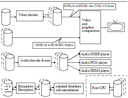
Fig.5: Application data flow to/from DDR
In this first description of the application , the DDR bandwidth (MBytes/s) requested by each IP are listed.
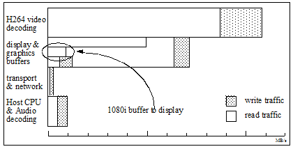
Fig.6: Relative DDR bandwith requirement per IP (HD Set Top Box application)
2 – IP traffic shape
After the budget specification of the application (in MBytes/s), the next step consists in specifying each IP traffic shape. The IP traffic shape can have 2 impacts on the SoC performance:
- Bus opcode size versus bus width:
- Bus opcode and burst length vs. DDR timing:
3 – DDR access timing: intrinsic overhead
The DDR protocol has an intrinsic timing overhead for accessing the data.
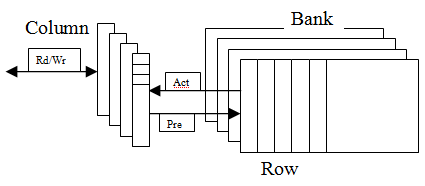
Fig.7: Internal DDR organization (bank/row/col)
The memory controller receives requests from the interconnect. It is in charge to drive the read/write commands to the multi-bank DDR and to interleave the bank commands (precharge/activate).

Fig.8: DDR Bank A and Bank B read sequences
In the above example, the idle cycles of the intrinsic timing are used, as much as possible by the memory controller to anticipate the next read/write command to the other banks by interleaving bank commands (precharge and activate).
III - Performance verification methods
The SoC performance verification process used mainly two methods. The first one is an analytical method based on a computation chart (spreadsheet). This method gives preliminary performance figures before any SoC implementation activity. The second one is based on simulations and gives more accurate performance figures but requires the design of a cycle-accurate interconnect model. The correlation between the two methods is essential to validate the results.
1 – Analytical and statistical model
The purpose is to determine the minimum DDR frequency to transfer the total bandwidth requested by the application.

A spreadsheet is set up to calculate the number of DDR cycles needed to achieve the traffic required by each IP. The inputs of the table are:
- The IP characteristics for the given application.
- The DDR timing specifications
Intrinsic timing of a burst
The intrinsic timing of a burst is the sum of each opcode intrinsic timing. The opcode intrinsic timing only depends on its size and the DDR bus width.
| opcode | DDR Intrinsic timing hypothesis: DDR bus width=32 bits |
| 32 bytes | 4 DDR cycles |
| 16 bytes | 2 DDR cycles |
| 8 bytes | 2 DDR cycles (*) |
(*) DDR2 rd/wr operation is 2 cycles min
Timing overhead for the next burst
A statistical model provides an estimation of the timing overhead for the next burst. This model takes into account the following parameters:
- The timing overhead for the next burst is different if the next IP traffic is in a different bank or in the same bank but in a different page.
- The timing overhead is different if the DDR data bus changes its direction or not (Read burst followed by a Read burst or by a Write burst and vice-versa).
- The timing overhead is different for long or short burst.
- The timing overhead is different if the opcodes of the burst are big or small.
At the end, the overhead is a function of the above parameters:

Once the timing of each IP burst has been estimated, the total DDR cycles for the traffic of this IP is calculated as follow:

Burst length is a number of Bytes
IP bandwidth is expressed in MBytes/s
Finally, the minimum DDR frequency is obtained by summing the DDR cycles used by all the IPs.
This method is an analytical method based on statistical modeling. The importance of this first verification is to provide a reference figure of what can be achieved by an ideal interconnect and an ideal DDR controller. It provides an early figure of the DDR clock frequency needed to achieve the targeted performance.
2 – Dynamic verification by simulation
The advantage of the simulation platform is to explore verification aspects that can not be seen with the previous analytical method such as the impact of the interconnect arbitration scheme and interconnect FIFO sizes.
Nevertheless, the simulation speed must be high enough to be able to explore many scenarios. These concerns have oriented the choice toward a verification platform based on SystemC models.
The goals of the platform are:
- Generate concurrent IP STBus traffics
- Use STBus/VSTNoC interconnect and memory controller cycle accurate models
- Simulate with an acceptable runtime to validate the application (in terms of traffic to the DDR)
- Check automatically that each IP meets its DDR bandwidth and latency requirements
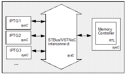
Fig.9: Dynamic verification platform
2.1 Components
2.1.1 Interconnect model
The interconnect model used in the simulation platform is a cycle-accurate SystemC model. This allows simulating accurately the IP traffics arbitration.
2.1.2 Memory controller and memory model
For the memory controller, an RTL or cycle-accurate SystemC model is used.
The memory model is not necessary since there is no handshaking between the controller and the DDR device.
2.1.3 IP traffic generators
The IPs traffics to the shared memory are modeled with traffic generators (IPTG). The model is written in TLM SystemC and configured by a text file for the customization of each IP. The model is based on a FIFO.
- For write initiators, the FIFO is filled by the IP and emptied by interconnect transactions.
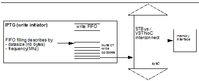
Fig.10: IP Traffic Generator for write initiators
- For read initiators, the FIFO is filled by the traffic from the interconnect and emptied by the IP
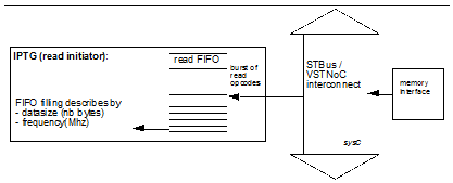
Fig.11: IP Traffic Generator for read initiators
The shape and sequence of the STBus transactions to the interconnect are described in a text file controlling the IPTG.
2.1.4 Constrained memory address generation
Each IPTG describes the STBus traffic with a sequence of addresses in a burst. A SystemC module is placed between the interconnect and the memory controller. Its function is to modify the address generation on the fly, to control the bank switch between 2 IP transactions (in a different page of the same bank or in a different bank)
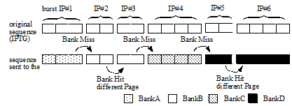
Fig.12: DDR address generation
2.2 Simulation
The simulation duration must be long enough to exercise all the IP traffics. During the simulation, the traffic generated by the initiators and received by the memory controller is probed in a VCD format.
The first benefit of the simulation is that it really exercises the arbitration between the different IPs with cycle accuracy. The second simulation benefit is that it creates a realistic IP traffic sequencing at the memory controller input. Interconnect arbitration weakness or memory controller limitations could impact the whole SoC performance compromising the final application. This would be identified during the simulation.
2.3 Check and results
The VCD file is post-processed to extract the average simulated bandwidth per IP and the whole bandwidth at the memory interface.
The traffic generator model embeds its own checker to identify if the real-time constraints have been met or not (FIFO overflow for write initiators, FIFO underflow for read initiators).
It is also checked that all the memory interface responses are granted immediately by the interconnect and that the interconnect does not stall the memory.
IV – Performance methods comparison and correlation with silicon
The two modeling methods have been used with different applications and scenarios. Results obtained with both methods have been compared. Also, the models results have been correlated with performance measurements of the silicon device running on the application board.
1 - Analytical and simulation results correlation
Two correlation methods have been used.
The first method consists in identifying and modeling a scenario saturating the DDR bandwidth with the analytical spreadsheet. The scenario is then run on the simulation platform to check if the scenario is passing. The table below gives the DDR frequency obtained with the two modeling methods. The difference is within 5%.
| Application | Spreadsheet estimated DDR frequency | IPTG simulation DDR |
| HDTV scenario 1 (with video recording) | f1 | PASS |
| HDTV scenario 2 (High quality video display) | f2 | PASS |
The second correlation method consists in using a DMA engine initiator having a low priority on the interconnect. For a given scenario, the memory bandwidths consumed by the DMA engine in the two modeling methods are compared. The table below gives the results obtained with the two methods. Given the current model characteristics, the analytical model is slightly more pessimistic than the simulation platform.
| Scenarios | IPTG simulation versus Statistical Model |
| Scenario 1 (Basic set –top box) | +8.9% |
| Scenario 2 (PVR set-top box) | +8.1% |
2 - Correlation with silicon device performance
It is essential to correlate also the predicted performance with real performance figures measured on the silicon device. This correlation is important to refine the models accordingly.
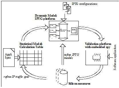
Fig.13: Refinement loop of the performance verification models
A bus analyzer is embedded inside the SoC to capture the traffic. These measurements allow qualifying the IP traffic in the real application which is orchestrated by a mix of hardware and software.
On the most memory-bandwidth demanding IP, the measurements have confirmed the prediction with an acceptable accuracy.
Conclusion
Performance verification of the SoC backbone {interconnect + memory controller} is essential to guarantee that the high memory-demanding IPs will get the memory bandwidth required by the application.
It is also important to start this performance verification activity in the early stages of the SoC design to confirm or update the SoC architecture.
The methods presented in this paper contribute to reach this objective.
Thanks to the other STMicroelectronics teams involved in performance verification area, and in particular to Davide Sarta, in STM-Bristol, Grégory Poivre, Stéphane Farrouch, Antoine Perrin in STM-Grenoble and STM OCCS team.
Related Semiconductor IP
- PUF FPGA-Xilinx Premium with key wrap
- ASIL-B Ready PUF Hardware Premium with key wrap and certification support
- ASIL-B Ready PUF Hardware Base
- PUF Software Premium with key wrap and certification support
- PUF Hardware Premium with key wrap and certification support
Related White Papers
- STBus complex interconnect design and verification for a HDTV SoC
- Reduce SoC verification time through reuse in pre-silicon validation
- Simplifying SoC Verification by communicating between HVL Env and processor
- Creating core independent stimulus in a multi-core SoC verification environment
Latest White Papers
- e-GPU: An Open-Source and Configurable RISC-V Graphic Processing Unit for TinyAI Applications
- How to design secure SoCs, Part II: Key Management
- Seven Key Advantages of Implementing eFPGA with Soft IP vs. Hard IP
- Hardware vs. Software Implementation of Warp-Level Features in Vortex RISC-V GPU
- Data Movement Is the Energy Bottleneck of Today’s SoCs