A design of High Efficiency Combo-Type Architecture of MIPI D-PHY and C-PHY
Ji-Hyun Kim, Jin-Yong Kim, Jae-Hyun Jeong, Eun-Ji Kim,Yong-Ju Cho and Ian Lee, LG Electronics, Seoul, Korea.
Abstract
MIPI C-PHY is suitable for mobile camera and display applications. In this paper, we proposed an effective active C-PHY driver scheme without any increase of the size and control pins. Additionally, C-PHY has many characteristics in-common with D-PHY because many parts of C-PHY were adapted from D-PHY. Therefore, we present a combo-type architecture of MIPI D-PHY and C-PHY. The presented architecture designed to operate both D-PHY and C-PHY sharing in-common blocks so that we can save the area and the I/O pins. In order to facilitate the architecture, we propose how the structure be designed. The presented design communicates data at the maximum rate of 5.7Gb/s and is verified in a standard FinFET CMOS technology.
Index Terms
MIPI, D-PHY, C-PHY, mobile camera application.
I. INTRODUCTION
As the required smartphone functionality increases, the amount of data that needs to be transferred is increasing steadily. Moreover, a low power consumption and a compacted size are becoming more important than before.
For mobile companies that need to design this system, MIPI Alliance offers a comprehensive interface standard between chipsets and peripherals in mobile connected devices. MIPI D-PHY is a serial interface technology using differential signaling for streaming applications such as displays and cameras. [1]-[4]. However, although differential signaling help the circuit consume efficiently power, it causes a pin efficiency drop of 50%. To deal with this issue, MIPI C-PHY is developed, it is based on the 3-Phase symbol encoding technology delivering 2.28 bits per symbol over three-wired trios, and promotes a pin efficiency by the use of tri-level signaling [5]-[6].

Fig. 1. Block Diagram of MIPI C-PHY
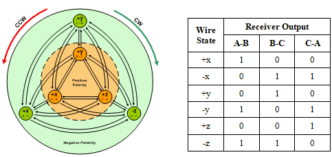
Fig. 2. Sate Diagram Showing All Six Wire States, and All Possible Transitions
Fig 1 shows all processes involved in the transmission of 16-bit data. 16-bit words at the transmitter are converted to seven symbols by a Mapper. Then the seven symbols are sent one symbol at a time to a Symbol Encoder. And then the encoded seven symbols are serialized and 3-wire driver which drives the three signals of the lane (A, B and C lines) at the transmitting end. At the receiving end, there are three differential receivers that A minus B, B minus C, and C minus A. The digital outputs of the differential receivers connect to a serial-to-parallel and a clock recovery circuit. Then the parallelized seven symbols are fed to a Decoder and covert a 16-bit word by a De-Mapper. Fig 2 illustrates six possible wire states and five possible state transitions. The symbol value is defined by the change in wire state values from one nit interval to the next. [5]
This paper proposes a new scheme to design C-PHY Transceiver without reflection and presents a combo-type architecture of 5.7 Gb/s C-PHY and 2.5 Gb/s D-PHY transceivers that consumes only 4.2mW each lane, resulting in a low area and I/O pins efficiency.
This paper is organized as follows, Section II introduces the proposed scheme, Section III presents combo-type architecture, and Section IV shows measurement results. Finally, Section V concludes this paper and gives some future research directions.

Fig. 3. Proposed Tri-level Driving Schemes
II. PROPOSED SCHEME
Simply, we can design passive mode tri-level driver. However, this method generates what we don’t want at high speed, for example, as shown Fig. 3(a), the current flows through only two channels, and other channel isn’t flowed the current, so the reflection that occurs negative effects appears at the unknown edge. In order to deal with this issue at high speed, typically we use the active mode. In this mode, the reflection disappear because the additional switches keep the middle level. But control pin increase two time than the passive mode, and additional switches occupy considerable area.
Fig. 3(c) presents the proposed active mode of tri-level driving scheme. The proposed technique implements differential structure without increase in size. This is because even though the number of the switches increases in two times, the resistance of each switch is reduced a half of one. Also, the number of the control pins can remain the same as the passive mode.
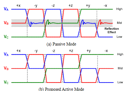
Fig. 4. Single-ended High Speed Signals
In detail, when operated as passive mode, an unknown channel edge generates the reflection effect and the range of the mid-level is increased. This can reduce the range of the operating voltage. Fig. 4 shows an improvement point of proposed active mode compared to passive mode.
III. COMBO-TYPE ARCHITECTURE
Fig. 5 shows a block diagram of the MIPI C-PHY and MIPI D-PHY interfaces. Both interfaces supports a high-speed (HS) for fast data transfer and also a low-power (LP) for control transactions. Fig. 5(a) shows D-PHY lane module that consists of a digital block for controls and an analog block for data transmission. And Fig. 5(b) presents C-PHY that has many characteristics in-common with D-PHY because many parts of C-PHY were adapted from D-PHY. Thus C-PHY was designed to be able to coexist on the same I/O pins as D-PHY [5]. Therefore, we proposed the combo type architecture that can be used both C-PHY and D-PHY sharing pins and some blocks.
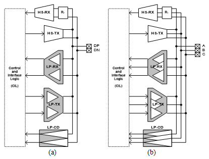
Fig. 5. Diagram of MIPI D-PHY (a) and C-PHY (b) modules
A. Low Power Mode
The proposed architecture of LP Mode is illustrated in Fig. 6. In the transmitter, digital logics of D-PHY and C-PHY is included in Control and Interface Logic (CIL). And digital switches (Mux) that place between CIL and Driver is controlled according to a selected mode. Transmitter’s drivers are shared with D-PHY and C-PHY. Meanwhile, in the Receiver, digital logics of D-PHY and C-PHY is also included in CIL. And digital switches (DeMux) that place between RX-Buffer and CIL is controlled according to a selected mode. Receiver’s drivers are shared with D-PHY and C-PHY.
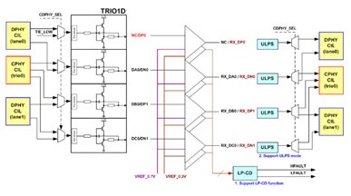
Fig. 6. Proposed Architecture of MIPI LP Mode
According to sharing I/O pins and drivers with C-PHY and D-PHY, this structure can reduce the size, and save the number of required I/O pins.
B. High Speed Mode
The proposed architecture of HS Mode is illustrated in Fig. 7. Like the way of LP mode, CIL includes TX/RX’s digital parts of D-PHY and C-PHY, and digital switches (Mux and DeMux) can be controlled according to a selected mode. While main drivers are designed as dual-type not sharing them because there is a difference between C-PHY and D-PHY, in specific, C-PHY is 3-wires system, and the signals have three level unlike D-PHY’s structure.
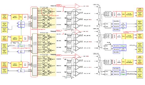
Fig. 7. Proposed Architecture of MIPI HS Mode
To deal with this issue, we proposed a dual type structure shown as Fig. 8. It can be easy to design this structure because it is similar to pseudo differential structure at D-PHY that has been used before. Also, each resisters at receiver side is connected the same number of lines from transmitter’s drivers. So it can reduce a mismatch effect. In detail, each transmitter has two identical drivers. Up-side drivers are used at D-PHY mode, and down-side drivers are used at C-PHY mode.
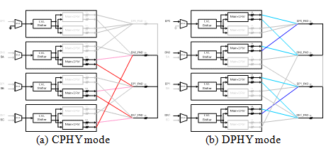
Fig. 8. Proposed Driver Structure
IV. MESUREMENT RESULTS
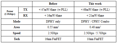
The MIPI transceiver was fabricated in 10-nm FinFET process. The prototype is shown in Fig. 9. The chip area is 0.475 mm2. Power consumption of MIPI C/D-PHY is 68 mW at 2.5Gb/s data rate.
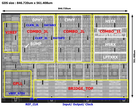
Fig. 9. Chip microphotograph
The size of proposed structure has decreased by 23% compared with the previous one, even though the proposed structure included C-PHY structure as well.
TABLE 1: PERFORMANCE COMPARISON
V. CONCLUSION
In this paper, we proposed an effective C-PHY driver scheme without increase of the size. Also, we present a combo-type architecture of MIPI D-PHY and C-PHY which is suitable for mobile camera and display applications. The presented architecture designed to operate both D-PHY and C-PHY sharing in-common blocks so that reduces area and saves I/O pins. We described how the proposed architecture be designed and how the circuit operates. Consequently, we expected techniques can be easily adopted for commercial products and the results prove their efficiency.
REFERENCES
[1] B. D. Kim, S. J. Lee, D. H. Kim, and K. R. Cho “Design of a D-PHY Chip for Mobile Display Interface Supporting MIPI Standard” IEEE ICCE, pp. 660-661, Jan. 2012.
[2] R. Lawrence, “High-speed serial interface for mobile displays,” in Proc.IDW, pp. 2013-2016, 2006
[3] MIPI alliance, “MIPI alliance specification for display serial interface, version 1.01.00,” 2008.
[4] MIPI alliance, “MIPI alliance specification for D-PHY, version 1.20.00,” 2014
[5] MIPI alliance, “MIPI alliance specification for C-PHY, version 1.00.00,” 2014
[6] W. J. Choi, T. W. Kim, J. J. Shim, H. S. Kim, G. H. Han, and Y. C. Chae “A 1V 7.8mW 15.6Gb/s C-PHY Transceiver Using Tri-Level Signaling for Post-LPDDR4” ISSCC 2017, pp. 402-403, 2017
Related Semiconductor IP
Related White Papers
- Demystifying MIPI C-PHY / DPHY Subsystem
- Analog switches in D-PHY MIPI dual camera/dual display applications (Part 1 of 2)
- Analog switches in D-PHY MIPI dual camera/dual display applications (Part 2 of 2)
- All you need to know about MIPI D-PHY RX
Latest White Papers
- Ramping Up Open-Source RISC-V Cores: Assessing the Energy Efficiency of Superscalar, Out-of-Order Execution
- Transition Fixes in 3nm Multi-Voltage SoC Design
- CXL Topology-Aware and Expander-Driven Prefetching: Unlocking SSD Performance
- Breaking the Memory Bandwidth Boundary. GDDR7 IP Design Challenges & Solutions
- Automating NoC Design to Tackle Rising SoC Complexity