Demystifying MIPI C-PHY / DPHY Subsystem
Tradeoffs, Challenges, and Adoption
Ashraf Takla, Mixel
The newest member of the MIPI® PHY family, the C-PHYSM, arrived in October 2014 to a mixture of excitement and apprehension. How would this new C-PHY compare to the MIPI D-PHYSM and M-PHY®? What would differentiate the C-PHY, and would it be compatible enough with the D-PHY so that both could coexist in a hybrid subsystem?
Now, years later, the answers are clear.
This article will lay out each of those answers, providing a high-level overview of both the D-PHY and C-PHY architecture, highlighting similarities and differences, identifying the pros and cons of each PHY, and providing insight into some of the challenges encountered while implementing the C-PHY. Finally, we will look at Mixel®’s innovative implementation of the C-PHY/D-PHY Combo IP, silicon results from multiple sources, cover uses cases, and examine the adoption of the C-PHY/D-PHY Combo solution in the market place.
Let's begin by taking a closer look at the D-PHY, which has been around since 2009, and thus better understood, and widely deployed. The D-PHY is a simple source synchronous PHY that uses one clock lane and a varying number of data lanes. The block diagram of the four-data lane D-PHY is shown in Figure 1 and the details of each lane are presented in Figure 2. Since the D-PHY has been in the market for almost a decade, there is an abundance of literature available covering its unique features and use-cases (1).
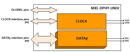
Figure 1: Four data lane D-PHY block diagram
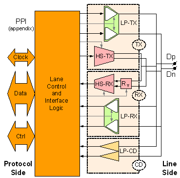
Figure 2: Block Diagram of a D-PHY data lane
In contrast, the C-PHY is a newer and more complex PHY. It operates on three signals, a trio, and the clock is embedded into the data, rendering a separate clock lane unnecessary. The block diagram of the C-PHY is shown in Figure 3 below.
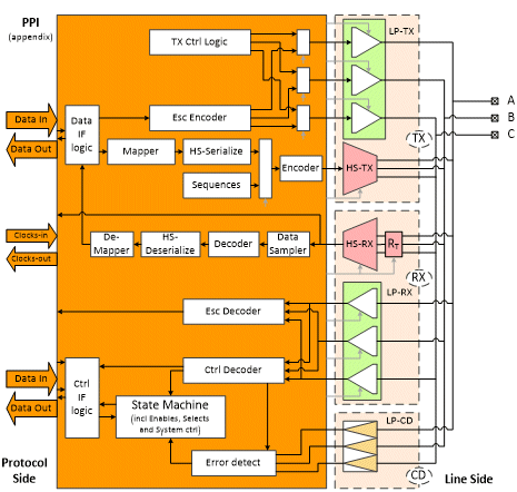
Figure 3: C-PHY Block Diagram
Table 1 compares between the D-PHY and C-PHY.
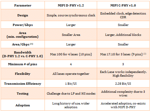
Table 1: C-PHY vs. D-PHY parameters comparison
Notes:
(1) Four data D-PHY lanes vs. three MIPI C-PHY trios
(2) Higher bandwidth due to Encoding
The C-PHY uses encoded data to pack 16/7 ≈ 2.28 bits/symbol, while the D-PHY does not use any encoding. Because of that, the C-PHY can achieve a higher data rate as compared to the D-PHY, while running at the same transition or symbol rate.
At first glance, the workings of the C-PHY, as well as a potential C-PHY/D-PHY combination, may seem mysterious. The C-PHY signaling is multi-level, but its receiver does not need to detect the difference between the multi-level! How can that be? How can the C-PHY and D-PHY, not only coexist, but be efficiently combined into one IP despite their clear differences? The D-PHY uses differential signaling, while the C-PHY uses a trio. Is it possible for them to work together? How can a combo C-PHY/D-PHY be efficiently implemented, using all the D-PHY building blocks, without any duplication? Where does the ratio 16/7 for the number of data bits per symbols come from? So many questions!
Let us attempt to answer these questions by first trying to demystify the C-PHY. Not an easy task!
In Figure 4 below, we provide a quick overview of the C-PHY. The block diagram in Figure 4(a) shows how a three-lane C-PHY TX and RX are connected. Figure 4(b) shows the different sub-blocks of a C-PHY sub-system, namely mapping, Parallel/serial function, encoding, and the channel. Figure 4(c) is a more detailed picture of the interaction between the TX and RX, and Figure 4(d), illustrates the C-PHY signaling levels.
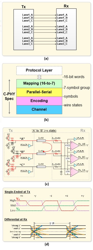
Figure 4: C-PHY (a) TX & RX connection, (b) different functions in C-PHY subsystem, (c) detailed TX & RX interaction, (d) C-PHY signaling levels at TX and RX outputs
A C-PHY lane is composed of a trio, A, B, and C as shown in Figure 4 (c) above. The C-PHY's receiver is made of 3 differential RX’s, each one looking at the difference between 2 of the 3 signals, (A-B), (B-C), and (C-A).
The C-PHY's encoder guarantees that (i) there is at least one edge/transition per symbol, (ii) that the differential input at all three RX’s is non-zero, and (iii) that the common mode of all 3 signals is constant. Item (ii) and (iii) above are achieved by restricting the combination of the TX signals during any single Unit Interval (UI) to high, mid, and low, and by keeping the voltage level on each of the three signals different. The combination of the three TX signal levels, high, mid, and low, that comply with restriction (i) above gives 6 different signal level combinations (wire states). The number of wire states, six, is the permutation of the three TX signal levels, 3! Additionally, the C-PHY encoder encodes the Flip, Rotate, Polarity symbol into a state changes based on the encoder rules.
To guarantee that there is at least one edge per symbol, item (i) above, the C-PHY must transition between different wire states as it moves from one symbol to the next and cannot stay at the same wire-state for two consecutive symbols. Because of that restriction, there are five different unique transitions between the six wire states. This means that the encoded data has five different possibilities i.e. each symbol has five possible states, making the C-PHY a base-5 system, or Quinary system. We are then moving between a binary system and a Quinary system. This why the C-PHY mapper is needed. Now that we are using a base-5 system, the maximum theoretical number of bits/symbol is log2(5) = 2.3219. The mapper function was constructed to enable the mapping ratio to be as close as possible without exceeding that theoretical limit. Additionally, the mapper must map between two integer numbers. The Ratio 16/7 ≈ 2.28 was chosen to achieve the above restrictions.
Another way to describe this is that the mapper needs to map 16 binary bits to a certain number of C-PHY symbols, but how do we determine how many symbol (S) do we map to? On the parallel interface there are 2^16 combinations and the combinations at the output of the mapper are 5^S => 2^16, so S = 7.

Figure 5: Overview of C-PHY encoding and mapping functions
To understand the reason why the C-PHY receiver only needs to detect the input signal polarity, and not the amplitude of the multi-amplitude signaling, we only need to remember that there is no data imbedded in signal amplitude. Multi-amplitude signaling is only utilized to increase the number of possible transitions and guarantee that there is least one transition per symbol.
One way to do an apple-to-apple comparison between performance of the C-PHY and D-PHY, is to compare them when they are supporting an aggregate data rate of 4.0 Gbps and operating at a similar transition rate. For D-PHY this can be accomplished by using four-lane D-PHY, using 10 wires, each Lane running at 1.0Gbps/lane. To obtain the same aggregate data rate at the same or lower transition rate with C-PHY, we can use two-lanes C-PHY, with 6 wires, running at 0.875Gsps, which is less than the 1.0Gsps for the D-PHY. In that case, the aggregate data rate for the C-PHY is 2 * 0.875 * 16/7 = 4Gbps. This comparison is shown in Figure 6 below.
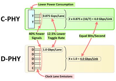
Figure 6: Comparison between D-PHY and C-PHY supporting 4Gbps aggregate data rate, and using same transition rate
Based on this comparison, the C-PHY has fewer wires (up to 40% less), lower Toggle Rate/Lane (12.5% lower), lower Power Consumption (~20-50% lower), a smaller number of lanes, thus smaller area for same Gbps, and no Emissions from a Clock Lane.
Thus when comparing the C-PHY and D-PHY at the same aggregate data rate, the C-PHY has many advantages; fewer pins and balls (due to higher performance per pin), flexibility, since each C-PHY lane is independent, with embedded clock, making it possible to borrow one lane from one link to another, while coexisting on the same pins with MIPI D-PHY. The C-PHY also allows lower power at higher data rate applications. Furthermore, C-PHY's embedded clock lane enables assignment of any lane on the Application Processor to any link, and eliminates clock spur emissions, which is particularly important in multi-band wireless devices.
C-PHY's embedded control codes also enable efficient support of emerging features such as fast Bus Turn Around (BTA) operations, lower latency (LRTE) for time-sensitive links, and Alternate Low Power mode (ALP), which would enable longer reach by eliminating single-ended LP mode, resulting in area reduction. Finally, the C-PHY's lower toggle rate often simplifies manufacturing and lowers costs of low cost products, such as low-end cameras.
Now that we have gone over the individual attributes of both the C-PHY and D-PHY, we can numerate some of the advantages of the C-PHY and D-PHY combo. This includes being able to share serial interface pins, reusing the LP (Low Power) mode, sharing of common blocks, resulting in area reduction, power/Gbps reduction, a smooth transition between MIPI D-PHY and MIPI C-PHY and taking advantage of MIPI C-PHY Power/Performance/area (PPA) improvements, while maintaining compatibility with MIPI D-PHY.
Mixel's implementation of C-PHY/D-PHY Combo IP is unique. All the D-PHY blocks are reused for C-PHY operation (HS-TX, HS-RX, SER, DESER, LP-TX, LP-RX and LP-CD), minimizing the area overhead for C-PHY support. While all blocks were reused, the Encoder, Decoder, CDR, Mapper and De-Mapper are additional blocks that are needed for C-PHY functionality. The block diagram of the Mixel implementation is shown in Figure 7 below.
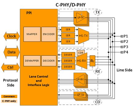
Figure 7: C-PHY/D-PHY combo IP block diagram
The Combo C-PHY/ D-PHY has been implemented in many different nodes and foundries by Mixel and Qualcomm as shown in Table 2.

Table 2: Nodes and foundries where the C-PHY/D-PHY combo IP has implemented by both Qualcomm and Mixel
S: Silicon-proven
P: Pre-silicon
Mixel and Qualcomm
Below we show the test setup and silicon evaluation for the C-PHY and D-PHY transmitters

Figure 8: MIPI C-PHY Transmitter Testing Set-up

Figure 9: Silicon Results: TX MIPI C-PHY – Eye Diagrams (Mixel)

Figure 10: Silicon Results: TX MIPI C-PHY – Eye Diagrams (Qualcomm)

Figure 11: Silicon Results: TX MIPI C-PHY – Eye Diagrams (Sony)

Figure 12: Silicon results: TX MIPI D-PHY – Eye Diagrams (Mixel)

Figure 13: Silicon Results: TX MIPI D-PHY – Eye Diagrams (Qualcomm)
Below we show the test setup and silicon evaluation for the C-PHY and D-PHY receiver

Figure 14: Silicon Results: RX MIPI C-PHY- Electrical (Qualcomm)

Figure 15: Silicon Results: RX MIPI C-PHY - Link (Qualcomm)

Figure 16: Example use case: camera bring up

Figure 17: Example use case: Display bring up
Now, let us look at the power, performance, and area, for different use-cases in current display and camera applications. These are shown in Table 3 below.
There is small area increase when comparing the D-PHY and C-PHY/D-PHY combo at the same data rate. The normalized power of the C-PHY only module, when compared at the same Gbps is comparable. The C-PHY has a clear advantage in enabling higher data rates than the D-PHY at the same transition rate.
However, the power increment combo PHY can be cancelled by enabling multiple design options in CPHY mode configuration (not shown here).

Table 3: PPA of different use-cases for Display applications
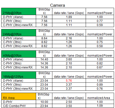
Table 4: PPA of different use-cases for Camera applications
Notes:
- Combo PHY area increment < 10%
- Combo PHY can cover wide range of Resolutions: 80Mpbs - 10Gbps - 17.1Gbps - 18Gbps - 23.94Gbps
- MIPI C-PHY mode: ~10-30% lower power than DPHY mode because of low frequency/ smaller bias / lesser # of lanes
- Courtesy of QUALCOMM
The C-PHY/D-PHY combo has gained wide adoption in multiple use-cases, by many different vendors, and in many different types of products, including camera (Sony, OVT, and others), display (interoperability testing completed with most Major DDIC companies). The ecosystem is supported by wide participation covering IP (Mixel), AP/SOC (Snapdragon and others), testers (Keysight, Tektronix, Introspect, The Moving Pixel Company), and common-mode filters (Murata, Panasonic, TDK).
The higher performance of the C-PHY does not come for free; however. There are challenges that come with the C-PHY, including a unique CDR that requires programming for different data rate rages, multi-level signal transmission, which introduces encoding jitter, and a unique trio-based signaling that complicates PCB design.
In conclusion, the MIPI C-PHY is a more complex, more powerful and efficient PHY and the C-PHY/D-PHY combo is even more so on all accounts. Mixel has created and silicon-proven the Dual Mode MIPI D-PHY/ MIPI C-PHY, enabling a smooth transition between the two PHY’s. Mixel’s Dual Mode MIPI D-PHY/ MIPI C-PHY shares all common blocks, resulting in area reduction, and reduced power/Gbps. It has the benefit of the MIPI C-PHY PPA improvements, while maintaining compatibility with MIPI D-PHY, and using the same serial interface pins. Furthermore, The MIPI C-PHY/MIPI D-PHY combo is silicon-proven in multiple nodes and foundries and has been integrated into several end products by many tier-one SOC, sensor, and display vendors. As we look forward, we see accelerating traction for MIPI C-PHY/MIPI D-PHY combo for camera application, while display applications catching up soon.
References:
Related Semiconductor IP
Related White Papers
- A design of High Efficiency Combo-Type Architecture of MIPI D-PHY and C-PHY
- Analog switches in D-PHY MIPI dual camera/dual display applications (Part 1 of 2)
- Analog switches in D-PHY MIPI dual camera/dual display applications (Part 2 of 2)
- All you need to know about MIPI D-PHY RX
Latest White Papers
- Ramping Up Open-Source RISC-V Cores: Assessing the Energy Efficiency of Superscalar, Out-of-Order Execution
- Transition Fixes in 3nm Multi-Voltage SoC Design
- CXL Topology-Aware and Expander-Driven Prefetching: Unlocking SSD Performance
- Breaking the Memory Bandwidth Boundary. GDDR7 IP Design Challenges & Solutions
- Automating NoC Design to Tackle Rising SoC Complexity