Linearity Analysis of Source-Degenerated Differential Pairs for Wireline Applications
By Kunal Yadav (University of Toronto), Ping-Hsuan Hsieh (National Tsing Hua University) and Anthony Chan Carusone (University of Toronto)
Abstract
This paper presents a comprehensive analysis of nonlinearities in differential pairs with source degeneration and their impact on wireline communication applications. We assess the suitability of three nonlinearity metrics to quantify the receiver analog front-end performance. This work identifies the primary sources of nonlinearity in differential pair circuits including, broadband Variable Gain Amplifiers (VGAs) and Continuous-Time Linear Equalizers (CTLEs) using circuit simulations. Furthermore, the linearity performance of different front-end configurations is evaluated, providing design insights. The analysis is validated through simulations with a 22-nm FDSOI technology.
INDEX TERMS
Continuous time linear equalizer (CTLE), analog-to-digital converter (ADC), pulse amplitude modulation (PAM), wireline transceiver.
I. Introduction
The growing demand for higher data rates in wireline communication links has driven the development of solutions that leverage multilevel signalling techniques. Specifically, pulse amplitude modulation (PAM) with 4 or more levels is used [1], [2], [3], [4], [5]. While PAM signals with more levels offer increased data rates, they also exhibit greater susceptibility to imperfections, such as residual intersymbol interference (ISI) and nonlinearity, when compared to PAM-2 signals. Various equalization techniques have been adopted to address ISI. While more power digital signal processing can reduce residual ISI, nonlinearity distorts the signal and cannot be repaired as easily. Thus, the nonlinear characteristics within these systems now critically limit their vertical eye opening, impairing their signal-to-noise ratio (SNR) and elevating their bit error rate (BER) [2], [6], [7].
Therefore, a critical need has arisen to evaluate and address nonlinearity in the analog front-end (AFE) of broadband wireline receivers. For instance, in [7], the linearity requirements of PAM-8 wireline transceivers were studied, and a nonlinearity cancelation technique was proposed to improve the front-end linearity. Similarly, in [6], the linearity requirements for broadband optical receivers were analyzed.
The source-degenerated amplifier architecture finds extensive use in wireline receiver front-ends due to good linearity, reconfigurability, and potential for bandwidths of 10’s of GHz [1], [2], [5], [8], [9], [10]. Fig. 1(a) shows a front-end design example with source degeneration in both the CTLE and VGA stages. Fig. 1(b) further shows an alternative CTLE design employing transadmittance-transimpedance amplifier (Gm-TIA, or TAS-TIS) architecture with a complementary degenerated differential input stage [1], [9], [10].
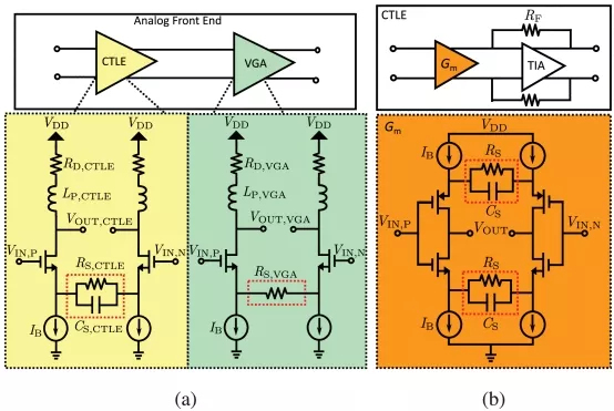
FIGURE 1: (a) CTLE and VGA design example employing differential pairs with source degeneration [5], [8]. (b) CTLE design example employing Gm-TIA architecture with degenerated differential input pair [1], [9], [10].
Source-degenerated amplifiers exhibit enhanced linearity due to the reduced signal swing between the gate and source of the input transistors. Nevertheless, to further augment the performance with the limited supply voltage in advanced technology nodes, particularly for high-speed PAM-modulation schemes, designers in [11] and [12] have opted to employ a higher supply for the AFE blocks. This affords extra voltage headroom and, consequently, boosts the front-end linearity. With the TAS-TIS topology, linearity is further enhanced by the feedback in the second stage, which reduces the voltage swing at the first stage output. Of course, the linearity of the second stage is impacted by its wider output swing and needs to be investigated.
In this work, we investigate the linearity characteristics of differential pairs with source degeneration and provide designers with tools and methods to consider linearity in designing wireline AFEs. In Section II, we discuss three common metrics used for assessing the linearity of AFEs for wireline links. We evaluate and correlate these metrics using the behavioral model. By evaluating the third harmonic distortion (HD3) on an example design in a 22-nm FDSOI technology, Section III investigates the factors contributing to nonlinearity in differential pairs with source degeneration and analyzes their incremental impact. Section IV extends the analysis to incorporate the broadband signal characteristics of VGA and CTLE circuits. Furthermore, Section V discusses the optimization of a complete AFE chain by considering the co-design of CTLE and VGA blocks. Finally, Section VI presents the summary and conclusions.
II. Metrics for Nonlinearity Evaluation
Evaluating nonlinearity in a wireline receiver is crucial to ensure the integrity of received PAM signals. This section explores the three metrics commonly used for assessing nonlinearity.
A. Single-Tone Test
The single-tone test entails applying a single sinusoidal signal (a tone) of known frequency and amplitude to the AFE and analyzing the AFE’s output response. For broadband circuits, the single-tone test needs to be repeated at frequencies across the entire bandwidth. The single-tone test allows for quick and easy evaluation of nonlinearity, both in simulation and in the lab. However, its relationship to the BER performance of a wireline link remains uncertain.
B. Level Separation Mismatch Ratio (RLM)
As briefly mentioned in Section I, nonlinearity in an AFE can adversely affect its output signal integrity by giving rise to varying separations between different PAM levels. The Level Separation Mismatch Ratio (RLM) measures the irregularity among eye openings in a PAM signal [13], [14]. The RLM is defined as:
where:

In these equations, V0 , V1 , V2 , and V3 represent the mean voltage levels of the PAM-4 symbols. The mid-range level, Vmid , is defined as:

An RLM value of 1 indicates that the separations between all levels are equal, signifying a perfectly linear system without any distortion. While RLM is typically used on the transmitter side to measure linearity performance, it can be used to evaluate the linearity of the receiver front-end. However, it is not applicable to situations where a circuit processes unequalized or only partially-equalized PAM signals.
C. Signal-to-Distortion Ratio (SDR)
SDR1 is another metric to assess the received signal quality, as defined in [13], [15]. SDR relies on a linear fit pulse response and linear fit error for gauging distortion in a broadband PAM signal. To compute the SDR, the linearly fitted pulse response is derived from AFE output data using the Minimum Mean Square Error (MMSE) method, denoted as:
Here, Y denotes the AFE output waveform matrix, X1 is the concatenated input symbol matrix, and P represents the linear fit pulse response matrix. The synthesized waveform is then obtained by multiplying the pulse response matrix with the known symbol pattern (PX1) . The difference between the synthesized waveform and the received output signal is quantified as the error (E) attributed to the non-linear characteristics of the AFE:

SDR is calculated using the formula:
where pmax signifies the maximum value of the fitted pulse response, and σe represents the standard deviations of error. SDR serves as a valuable indicator, encapsulating the ratio between signal energy and noise arising from nonlinearity. It stands out as a key parameter aiding designers since it is evaluated using broadband and possibly unequalized signals. However, evaluating it requires longer simulations or more sophisticated measurement equipment in the lab.
To establish a relationship among the aforementioned metrics, all three were evaluated in the presence of a static third-order nonlinearity, α1x+α3x3 . For the single-tone test, a sinusoid is applied, and its frequency is irrelevant since no dynamic nonlinearity is included. For both the RLM and SDR tests, a PAM-4 PRQS-13 (Pseudo-Random Quaternary Sequence-13) pattern is applied to the non-linear block. The nonlinearity of the system was swept by varying the third-order coefficient value α3 while setting the linear gain α1 to 1, as illustrated in Fig. 2(a).
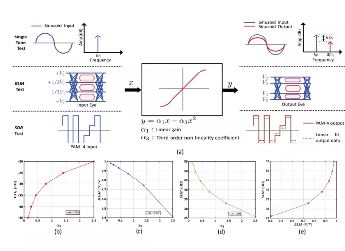
FIGURE 2: (a) Different test configurations to assess HD3, RLM and SDR metrics of nonlinearity (b) Single-tone test results for different α3 values (α1=1 ) showing third harmonic distortion (HD3) , (c) Level Separation Mismatch Ratio (RLM) results, (d) Signal-to-distortion result under different levels of nonlinearity. (e) Relationship between RLM and SDR for the specified α3 values.
As α3 increases, linearity degrades, and the third harmonic distortion (HD3) increases, as shown in Fig. 2(b). Additionally, the outer eyes of the PAM-4 output data compress, leading to a decrease in RLM, as shown in Fig. 2(c). The SDR value also decreases, as shown in Fig. 2(d). Fig. 2(e) plots the relationship between SDR and RLM for the third-order static nonlinearity. Small changes in RLM above 0.8, where most wireline AFEs operate, result in significant changes in SDR, making it a sensitive metric for quantifying AFE linearity.
III. Nonlinearity Contributing Factor in Differential Pair with Source Degeneration
In this section, we investigate the relationship between the nonlinearity of individual transistors and the overall nonlinearity of a source-degenerated differential pair, as depicted in Fig. 3. The primary factors influencing its linearity include: a) transconductance nonlinearity of the input-pair (M1,2) , b) variations in transistors’ drain-source node voltages (vds) , and c) variations in the voltage across the tail current source (M3,4) . Our analysis begins with the resistively degenerated differential pair in a VGA and will be extended to the CTLE by incorporating a degeneration capacitance, as discussed in Section IV.
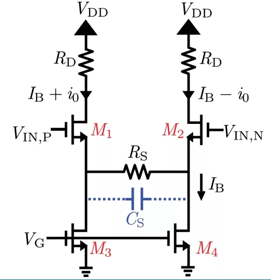
FIGURE 3: Differential pair with source degeneration.
For simulations, we employ a very low threshold voltage N-type MOS in 22-nm FDSOI technology, with a fixed gate length of 20 nm. With a fixed current, MOS width (and thus gm ) and degeneration resistance (RS) are systematically varied to manipulate the differential pair’s effective transconductance (Gm,eff) . The MOS finger width is fixed at 350 nm, while the number of fingers is adjusted to modify the overall transistor width.
With a supply voltage of 1 V, the input common-mode voltage (VCM) is set to 700 mV. Initially, we perform the linearity analysis at low frequency using a single-tone test. Specifically, a sinusoidal signal with a peak-to-peak voltage of 400 mVppd at a frequency of 1 MHz is applied to the input, and the third harmonic distortion (HD3) in the differential output current is calculated. Although not as accurate as other methods for evaluating broadband linearity, the quick simulation time of HD3 tests is helpful for rapid design-space exploration over a wide range of circuit parameter values. For comprehensive broadband linearity analysis, an SDR test will be conducted in Section IV.
To provide the design insight necessary to optimize transistor sizing and biasing, we perform a series of simulations to isolate different sources of nonlinearity in Fig. 3.
A. Transconductance Nonlinearity
Nonlinearities in the input transistors’ transconductance result in nonlinearities in the output drain current [16], [17]. The differential circuit of Fig. 3 is modified to focus on this particular nonlinearity. A fixed tail current is maintained using an ideal current source (IB=2.5 mA). Additionally, as illustrated in Fig. 4(a), a voltage-controlled voltage source (VCVS) with unity gain is introduced between the source and drain terminals of M1 to maintain a constant VDS,1,2 of 0.5 V.
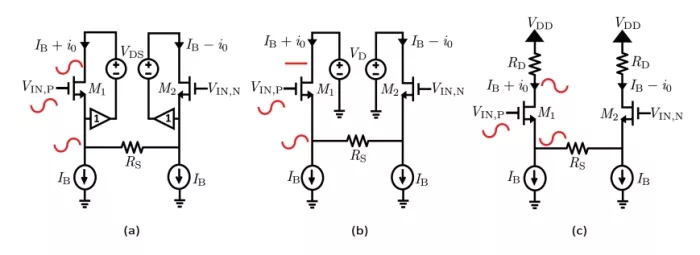
FIGURE 4: Different configuration of source-degenerated differential pair: (a) Employing VCVS between drain and source nodes, (b) Keeping the drain node at a fixed voltage, (c) Incorporating load resistance between supply and drain nodes.
Assuming a square-law model for the transistors, the effective transconductance and the HD3 of the source-degenerated pair are expressed as [17], [18]:
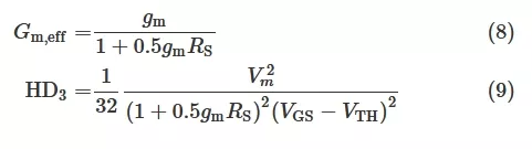
In these equations, gm denotes the small-signal transconductance of the input MOSFETs M1,2 , and Vm in (9) indicates the maximum input signal amplitude. Despite the limitation of the square-law model, it is still useful for understanding the nonlinearity trend in the SPICE simulation presented next.
Fig. 5 illustrates a 2-D contour plot of the SPICE simulated output current HD3. The black dashed lines denote the constant effective transconductance contours (Gm,eff) , and solid lines signify constant degeneration (1+0.5⋅gm⋅RS) . As we transverse from the lower left to the upper right corner, the degeneration increases, resulting in improved linearity. In the plot, if we increase RS while keeping gm constant (as indicated by the red horizontal arrow), the linearity improves as the degeneration increases, aligning with the trend outlined in equation (9). When we keep RS constant and increase gm by increasing transistor width (as indicated by the dashed yellow arrow), initially, third-order harmonic distortion decreases because the denominator of (9) increases. However, continuing to increase transistor width eventually pushes the input transistors into the more nonlinear subthreshold region, where the nonlinearity is not captured by (9).
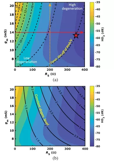
FIGURE 5: Color contour plot illustrating third-order harmonic distortion in a source-degenerated differential pair for varied gm and RS configurations (VCVS). The index lines in (a) show constant effective transconductance Gm,eff , and the solid line in (b) show constant degeneration (1+0.5⋅gm⋅RS) .
B. Impact of vDs Variation
In the presence of significant output voltage swing and small drain-source bias voltages, the nonlinearity stemming from the drain-source voltage variation (vds) becomes more pronounced [19], [20]. Large variations can even push the input differential pair out of the active region. Notably, in the case of the source-degenerated pair in Fig. 3, the drain and source node of the input MOS experience swings in opposite directions, exacerbating this variability.
To assess the influence of varying drain-source voltages, we consider two scenarios that generally mimic TAS-TIS and resistively-loaded differential pairs, along with the VCVS configuration presented in the previous subsection. First, we fix the voltage of the drain node of M1 at 700 mV to emulate the first stage of a TAS-TIS design [1], [2], as shown in Fig. 4(b). Second, we introduce a load resistance of 120 Ω between the power supply and the M1,2 drain nodes, resulting in an output common-mode voltage of 700 mV, as depicted in Fig. 4(c).
Figs. 5(a) and 6 (a-b) present 2-D contour plots of the HD3 in the output current for the three configurations with varied gm and RS settings. Upon examination, it becomes evident that when configured with identical gm and RS settings (indicated by the red star points), the more swing appears across vds1,2 , the greater the nonlinearity. Note that the HD3 contour plot of the output voltage is identical to the output current HD3 plot due to the linear resistance RD .
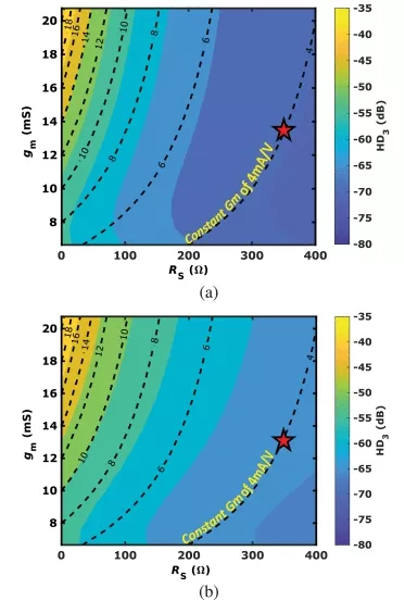
FIGURE 6: Contour plots illustrating third harmonic distortion for various vds configurations of a source-degenerated differential circuit under different gm and RS conditions. (a) Keeping the drain node fixed, (b) Incorporating load resistance between supply and drain nodes.
Fig. 7 shows the output distortion of a source-degenerated differential pair with fixed Gm,eff=6 mS (where gm=15 mS and RS=200 Ω ), while RD in Fig. 4(c) is varied to modify vds across M1 and M2 . VDD is adjusted to keep a constant VDS bias across MOS M1,2 . The results confirm that as the vds swing increases, the linearity degrades.
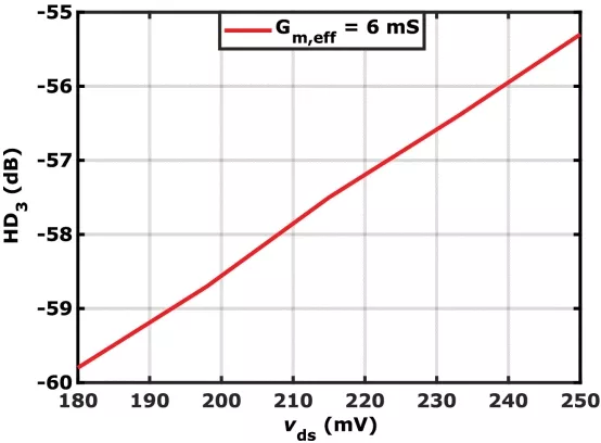
FIGURE 7: Third harmonic distortion result for a fixed Gm,eff and varying vds values.
Thus, circuit designers should minimize vds variations to enhance linearity. In existing literature, designers have mitigated the vds variations by using the TAS-TIS topology [1], [2], [21]. In [3] and [22], separate higher power supplies are adopted for the AFE to improve voltage headroom, allowing for greater vds swing.
C. Impact of Tail Current Source
In this subsection, we investigate the effect of the tail current source on the linearity of the source-degenerated differential pair. Whereas an ideal tail current source was used previously, we introduce MOS transistors M3 and M4 , as depicted in Fig. 8, while keeping the same bias conditions and load as in previous subsections (VDD=1 V, VCM= 700 mV and RD=120 Ω ). The tail MOS transistors are biased using a current mirror with a mirroring ratio of 10 (Ibias=250 μA , IB=2.5 mA and VD,sat,M3,4= 100 mV). The channel length of the tail MOS transistors is set to 60 nm to achieve higher drain-source resistance.
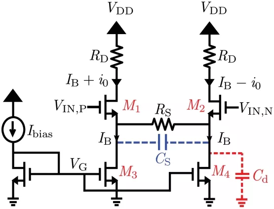
FIGURE 8: Source-degenerated differential pair including a tail current source.
Figure 9(a) presents a 2-D contour plot of the third harmonic distortion of the output voltage, highlighting the impact of the tail current source on the linearity of the source-degenerated differential pair. For a constant transconductance (gm) , indicated by the dashed pink arrow, the plot reveals a pronounced sweet spot in the circuit’s linearity that is not observable in the simulations with an ideal current source. For low values of RS , the linearity is predominantly influenced by the input transistors (M1,2) . However, with RS>200 Ω , linearity becomes predominantly influenced by the tail transistors (M3,4) due to growing swing in the voltage at their drain node (vDM3,4) . Notably, in the vicinity of 200 Ω , there is a dramatic increase in linearity attributable to the intricate interaction between M1 and M3 nonlinearities.
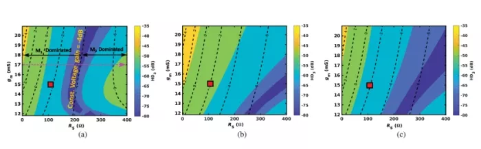
FIGURE 9: (a) Contour plot displaying third-order harmonic distortion patterns across different gm and RS settings after the inclusion of tail current sources M3 and M4 . The black dashed line represents the constant voltage gain from input to output. (b) Contour plot under a higher input common mode voltage (VCM= 800 mV). (c) Contour plot with both higher input common mode voltage (VCM= 800 mV) and supply voltage (VDD=1.1 V).
One way to mitigate the impact of M3,4 nonlinearity is to raise the input common-mode voltage level. By increasing VCM , the bias voltage at the drain nodes of M3,4 increases, thereby improving their bias margin. In simulations, when we elevated the input common-mode voltage from 700 mV to 800 mV, the contour plot shifts to the right, as depicted in Fig. 9(b). However, increasing VCM pushes M1,2 closer to the triode region. Thus, in regions where linearity is dominated by M1 , increasing VCM for the same gm and RS (as indicated by the red square points in Fig. 9 (a) and (b)) worsens linearity.
To improve linearity in the region dominated by the M1 transistor while using a higher input common-mode voltage, an effective approach is to increase the supply voltage. This increase improves the bias margins of the input transistors. In our simulations, when we increased the supply voltage from 1 V to 1.1 V, we observed an improvement in linearity, as shown by comparing the red square points in Fig. 9(c) with Fig. 9(b), though there was no significant improvement compared to Fig. 9(a). Moreover, increasing the supply voltage has increased the circuit’s power consumption.
Before transitioning to the wideband analysis in Section IV, the findings from the low-frequency analysis suggest a few design considerations for enhancing the linearity performance of the differential pair:
-
Ensure sufficient bias margin across the input pair and the tail MOS transistors to allow for high degeneration.
-
Minimize vds variations across the input pair transistors.
-
Increase the output resistance (rout) of the tail MOS transistor, as this resistance operates in parallel with RS , affecting the degeneration level.
IV. Broadband Linearity Analysis of Source-Degenerated Differential Pair
Whereas in the previous section, we assessed the static linearity of VGAs using a single-tone test at a low frequency of 1 MHz, this section investigates the broadband linearity of a source-degenerated differential pair circuit in both VGA and CTLE configurations using the SDR test.
A. Variable Gain Amplifier (VGA)
Simulations using a PRQS-13 input signal with a peak-to-peak amplitude of 400 mV at a baud rate of 56 Gbaud/s are performed to evaluate SDR, capturing both static and dynamic nonlinearity. The bias conditions and load settings are consistent with the previous subsections (VDD=1 V, VCM= 700 mV and RD=120 Ω ). Fig. 10(a) presents the SDR contour plot across various configurations of the input transistors’ gm and source degeneration resistance RS .
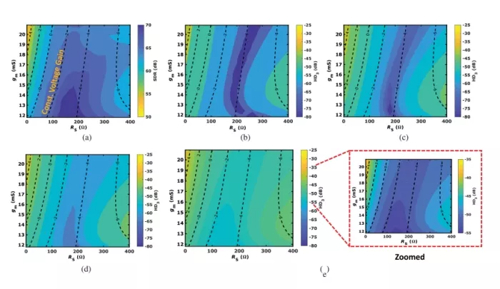
FIGURE 10: (a) Contour plot displaying SDR test results for VGA across different gm and RS settings. (b) through (e) present the contour plots illustrating the third harmonic distortion patterns of the VGA output for various gm and RS settings at different sinusoidal input frequencies: (b) 0.001 GHz, (c) 1 GHz, (d) 3 GHz, and (e) 9.33 GHz.
For comparison, Fig. 10(b) to Fig. 10(e) show the HD3 contour plots at different sinusoidal input frequencies. Significant differences can be observed between the SDR and HD3 contours at different frequencies. The differences are attributed to impedance, such as junction capacitance’s, that vary with signal fluctuations and the frequencies of interest [23], [24]. The SDR test captures both static and dynamic nonlinearities resulting from these variations in junction capacitance.
The results demonstrate that at higher input frequencies, the sweet spot in linearity is not as pronounced because reduced signal swings mitigate nonlinearity cancelation between the input and the current source transistors. Notably, the third harmonic distortion plot at 9.33 GHz in Fig. 10(e) follows contours with similar shapes as the SDR plot in Fig. 10(a).
These observations highlight the importance of conducting an SDR test or multiple single-tone tests at different frequencies to gain a comprehensive understanding of the VGA’s broadband linearity performance.
B. Continuous Time Linear Equalizer (CTLE)
In wireline receivers, CTLEs perform channel equalization by amplifying the high-frequency signals. Their high-pass frequency response is achieved using a differential pair with RC degeneration. By shorting the degeneration resistor, RS , at high frequencies, the degeneration capacitance CS in Fig. 8 can increase the high-frequency response of the differential pair by a boost factor of up to 1+0.5⋅gmRS .
To assess the CTLE’s linearity, we introduce a channel before the CTLE stage, as shown in Fig. 11(a). The channel loss is set to the maximum boost the CTLE is able to provide at each gm and RS combination, and the CS value is adjusted to produce a flat magnitude response for the combination of the channel and CTLE.
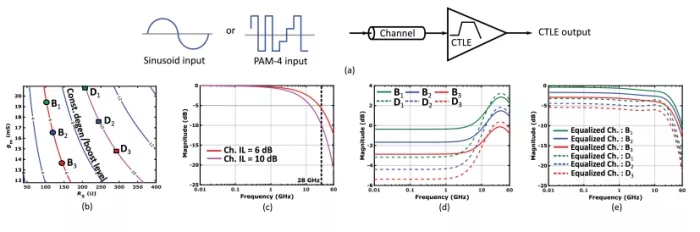
FIGURE 11: (a) Setup for CTLE linearity evaluation (b) CTLE degeneration/boost curves for different gm and RS values. (c) Channel insertion loss profile. (d) Frequency response of CTLE at selected points on the boost curves. (e) Post-equalization frequency response.
While it is common to have residual ISI after the CTLE stage or to adopt two CTLE stages for an even higher boost in high-speed wireline receivers, we strive for an apples-to-apples comparison across different CTLE design points. By maintaining a constant insertion loss profile for a given boost level, this procedure eliminates the influence of varying channel conditions on the results.
Fig. 11(b) illustrates the contours of the constant CTLE boost factor (1+0.5⋅gmRS) at different gm and RS values. For example, we have highlighted 6 dB and 10 dB boost levels in the design space, and the corresponding channel insertion loss profiles are presented in Fig. 11(c). For each specified boost level, three configurations with varying DC gains are selected. Fig. 11(d) shows the CTLE’s frequency responses, and Fig. 11(e) shows the post-equalization frequency responses accordingly.
The wideband linearity of the CTLE is evaluated with SDR tests by feeding a PRQS-13 signal at the channel input. The input signal has a peak-to-peak amplitude of 800 mV, and the data rate is 56 Gbaud/s. Fig. 12(a) presents the SDR contour plot across different (gm , RS ) settings. Additionally, Fig. 12(b) to (e) presents the HD3 contour plots at different sinusoidal input frequencies.
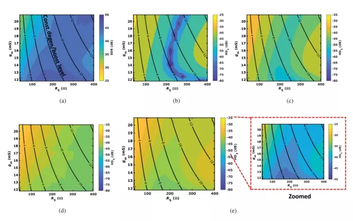
FIGURE 12: (a) Contour plot showing SDR test results for the CTLE across different gm and RS settings. (b) through (e) Contour plots depicting third order harmonic distortion patterns of the CTLE output at different input frequencies: (b) 0.001 GHz, (c) 1 GHz, (d) 9.33 GHz, and (e) 3 GHz. Solid lines are constant (1+0.5⋅gmRS) contours.
Similar to VGA analysis results, significant differences can be observed between the SDR and single-tone tests at different frequencies, attributed to impedance variations across the broadband signal fluctuations and signal bandwidth. Again, single-tone tests with higher input frequencies show shallower profiles across the design parameters. For the CTLE, the HD3 results at 3 GHz exhibits trends similar to the SDR plot, with both indicating a region of high linearity in the lower-middle section of the contour plot. The specific frequency at which the HD3 results will accurately predict SDR depends on the signals’ spectral characteristics and the specific circuit configuration.
We further evaluate the level separation mismatch ratio at the CTLE output across the design settings, as shown in Fig. 13. The results indicate that RLM degrades towards the upper-left corner of the plot, agreeing with the SDR results in Fig. 12(a). However, while Fig. 12(a) shows slight linearity degradation at the far-right side with large RS values, it is not apparent in Fig. 13. This discrepancy arises because RLM captures static nonlinearity, whereas SDR accounts for both static and dynamic nonlinearities [25].
FIGURE 13: Contour plot illustrating the RLM of CTLE output data across different gm and RS values.
The VGA and CTLE linearity analysis in this section highlights the limitations of using harmonic distortion and RLM evaluation alone. Although single-tone tests are straightforward and provide a quick assessment, multiple frequencies should be considered for a thorough evaluation across the bandwidth of interest. SDR offers a comprehensive understanding of the circuits’ broadband linearity performance but requires a longer simulation.
V. CTLE VGA Co-Design
In this section, we consider the co-design of the blocks in an AFE chain for a wireline receiver, with a specific focus on overall linearity performance. As shown in Fig. 14(a), the received signals are often conditioned by a CTLE and a VGA before being processed by either an ADC in DSP-based receivers or a DFE in analog receivers [1], [2], [3], [26], [27]. Two distinct AFE design scenarios are considered. The first scenario examines the linearity performance with a fixed CTLE design while varying the VGA configurations that provide the same gain. The second part extends the scenario to compare different CTLE designs and the corresponding VGAs under a fixed boost requirement.
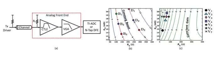
FIGURE 14: (a) Architecture of wireline receiver front-end. (b, c) Contour plots for CTLE boost level and VGA gain across different gm and RS values. Labels are shown for the design points in Section V.
A. Scenario #1: Fixed CTLE Design with Different VGAs
In this scenario, we evaluate the linearity performance of the AFE chain with a fixed CTLE design, as shown with the point of B2 in Fig. 14(b). With a channel loss of 6 dB at the Nyquist frequency of 28 GHz, the CTLE is configured to provide a 6-dB boost and a low-frequency gain of −2 dB. For a front-end DC gain of −1 dB, the following VGA is required to provide a 1 dB gain. Different VGA configurations corresponding to V1 , V2 , V3 , and V4 design points in Fig. 14(c) are examined. As shown with the frequency response in Fig. 15, the combinations of CTLE B2 with different VGA designs achieve almost the same overall AFE transfer function.
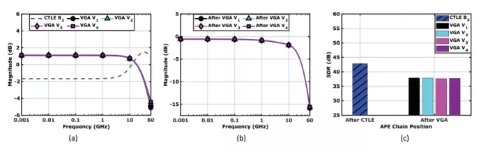
FIGURE 15: Scenario #1: (a) Frequency response of CTLE at design point B2 and VGA at design points V1 , V2 , V3 , and V4 . (b) Frequency response of AFE chain. (c) SDR test results.
SDR tests are conducted using a PRQS-13 signal at the channel input. The input PAM-4 signal has a peak-to-peak amplitude of 800 mV, and the data rate is 56 Gbaud/s. Our findings, shown in Fig. 15(c), reveal a degradation in linearity as the signal progresses through the CTLE and VGA. Despite the various VGA configurations, the overall AFE linearity performance remains relatively constant. This consistency aligns with our expectations, as the linearity performance along the VGA’s 1-dB gain contour line is similar, as shown in Fig. 10(a).
B. Scenario #2: Different CTLEs with Same Peaking Level
In this second part, with the same 6-dB-loss channel, we consider different CTLE designs with the same boost of 6 dB, but with different DC gains. The corresponding design points are shown as B1 , B2 , and B3 in Fig. 14(b). The CTLEs completely equalize the channel, and the following VGAs are then configured to points V5 , V6 , and V7 in Fig. 14(c) accordingly to ensure a consistent signal amplitude at the AFE output. The overall responses of the AFE chains are provided in Fig. 16(b), showing almost identical transfer functions.
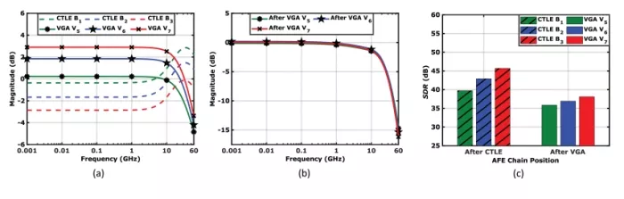
FIGURE 16: Scenario #2A (6-dB peaking): (a) Frequency response of CTLEs (B1 , B2 , and B3) and VGAs (V5 , V6 , and V7) . (b) Frequency response of AFE chain. (c) SDR test results.
SDR test results are shown in Fig. 16(c) and summarized in Table 1. We also repeat the same analysis for the 10-dB-boost CTLE design points of D1 , D2 , and D3 with a 10-dB loss channel. The corresponding results are shown in Fig. 17.
TABLE 1 SDR Test Results for Different AFE Configurations
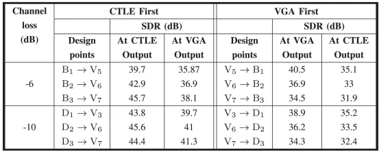
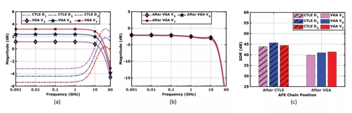
FIGURE 17: Scenario #2B (10-dB peaking): (a) Frequency response of CTLEs (D1 , D2 , and D3) and VGAs (V3 , V6 , and V7) . (b) Frequency response of AFE chain. (c) SDR test results.
For both the 6-dB and 10-dB boost tests, the overall AFE transfer functions are similar across different CTLE design points. The AFE configurations with the best linearity are those with a lower DC gain in the CTLE, followed by a higher gain in the VGA. The lower input amplitude to the VGA compensates for its worse linearity performance with a higher DC gain. Whereas this paper focuses on the linearity of the AFE, it is recognized that different design trade-offs impact the AFE’s noise performance, which should also be considered.
We also evaluated the linearity performance of an AFE with the VGA placed in front of the CTLE, as shown in Fig. 18(a). SDR tests for both 6-dB and 10-dB peaking design points are conducted for linearity assessment, with results presented in Fig. 18(b) and Fig. 18(c) and summarized in Table 1. The results show that placing the VGA before the CTLE degrades linearity due to signal amplification at the VGA output, adversely affecting both the VGA and CTLE performance. Furthermore, this AFE configuration exhibits a progressive decline in linearity across the three design points, with increasing VGA gains in both the 6-dB and 10-dB peaking scenarios, as shown in Fig. 18(b) and (c). This trend contrasts with the observations in Fig. 16(c) and Fig. 17(c).
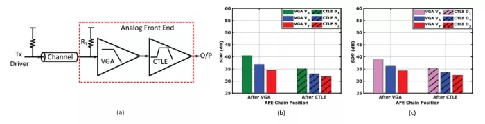
FIGURE 18: (a) Receiver AFE architecture with VGA as the initial stage, followed by a CTLE. (b) SDR test results with the CTLE configured to a 6-dB peaking setting (c) SDR test results with the CTLE configured to a 10-dB peaking setting.
Finally, Fig. 19 presents a 56 Gbaud/s AFE output eye diagram comparing the CTLE-first and VGA-first configurations. In this setup, the CTLE is configured at design point D3, and the VGA at design point V7, providing an illustrative comparison of eye quality between the two configurations.
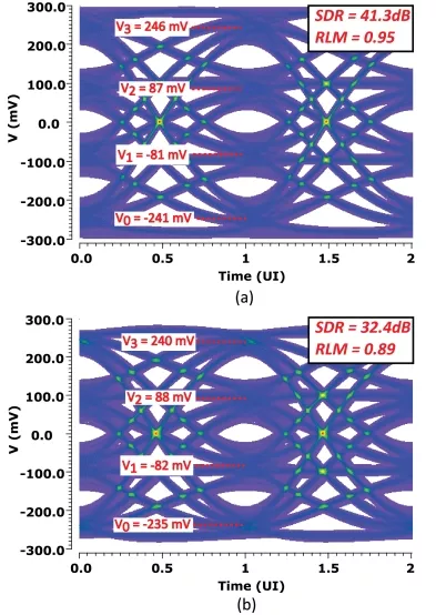
FIGURE 19: AFE output eye diagram: (a) CTLE configured at design point D3, followed by VGA at design point V7; (b) VGA configured at design point V7, followed by CTLE at design point D3.
VI. Conclusion
In this paper, we analyze the linearity of the source-degenerated differential pair circuit in the context of wireline receiver front-ends. Although more complex than simulations of HD3 and RLM, SDR tests help designers understand the impact of both static and dynamic nonlinearities in wideband circuits.
Circuit simulations demonstrate that increasing source degeneration enhances linearity until nonlinearity in the tail current source begins to dominate the performance. A higher input common-mode voltage, along with a higher supply voltage, helps reduce the impact of the tail current source on linearity. The results also suggest reducing the drain-source voltage swings, vds , across the input pair transistors. The use of TAS-TIS architectures helps reduce vds swing on the input transistors, affording additional flexibility in the design of AFEs.
Wideband linearity performance evaluation using SDR tests is performed for VGA and CTLE designs with source-degenerated circuit structures. Our analysis further reveals the limitations of single-tone test at a specific frequency. For a quick performance assessment, multiple single-tone tests at different frequencies are recommended.
Finally, we analyze the co-design of the functional blocks in the AFE chain for a wireline receiver, with a specific focus on overall linearity performance. We evaluate various scenarios involving different CTLE and VGA configurations. Even when designing for similar overall frequency responses, there are optimal AFE configurations from a linearity perspective. For example, placing the CTLE before the VGA in the AFE chain is found to help maintain better linearity.
Authors

Edward S. Rogers Sr. Department of Electrical and Computer Engineering, University of Toronto, Toronto, ON, Canada
Kunal Yadav (Graduate Student Member, IEEE) received the B.Tech. degree in electronics and communication engineering from Kurukshetra University, India, in 2011, and the M.Tech. degree in electrical engineering from the Department of Electrical Engineering, Indian Institute of Technology Hyderabad, Hyderabad, India, in 2016. He is currently pursuing the Ph.D. degree with the Edward S. Rogers Sr. Department of Electrical and Computer Engineering, University of Toronto. He worked as a Design Engineer II with Cadence Design Systems, Bengaluru, India, from 2016 to 2018.

Department of Electrical Engineering, National Tsing Hua University, Hsinchu, Taiwan
Ping-Hsuan Hsieh (Member, IEEE) received the Ph.D. degree in electrical engineering from the University of California at Los Angeles in 2009. She was with the IBM T. J. Watson Research Center, Yorktown Heights, NY, USA, from 2009 to 2011, and she joined the Electrical Engineering Department, National Tsing Hua University, Hsinchu, Taiwan, in 2011, where she is currently an Associate Professor. Her research interests include mixed-signal IC designs for high- speed electrical data communications, clocking and synchronization systems, and energy-harvesting systems. She served the Technical Program Committee of ISSCC. She is currently a member of the Technical Program Committees of A-SSCC and CICC. She served as an Associate Editor for IEEE Internet of Things Journal from 2014 to 2018 and a Guest Editor for IEEE Journal of Solid- State Circuits Special Issue in 2021, and is currently an Associate Editor for IEEE Open Journal of Circuits and Systems and IEEE Solid- State Circuits Letters

Edward S. Rogers Sr. Department of Electrical and Computer Engineering, University of Toronto, Toronto, ON, Canada
Anthony Chan Carusone (Fellow, IEEE) received the Ph.D. degree from the University of Toronto in 2002.
He has been a Professor with the Department of Electrical and Computer Engineering, University of Toronto. He has been a Consultant to industry in the areas of integrated circuit design and digital communication since 1997. He is currently the Chief Technology Officer of Alphawave Semi. He co-authored the Best Student Papers at the Custom Integrated Circuits Conferences in 2007, 2008, 2011, and 2022 respectively, the Best Invited Paper at the 2010 Custom Integrated Circuits Conference, the Best Paper at the 2005 Compound Semiconductor Integrated Circuits Symposium, the Best Young Scientist Paper at the European Solid-State Circuits Conference in 2014, and the Best Papers at DesignCon in 2021 and 2023, respectively. He was a Distinguished Lecturer for the IEEE Solid- State Circuits Society from 2015 to 2017 and has served on the Technical Program Committee for several IEEE conferences including the International Solid-State Circuits Conference from 2016 to 2021. He co-authored the popular textbooks “Analog Integrated Circuit Design” (along with D. Johns and K. Martin) and “Microelectronic Circuits,” (8th Ed., along with A. Sedra, K. C. Smith and V. Gaudet). He was an Editor-in-Chief of the IEEE Transactions on Circuits and Systems II: Express Briefs in 2009, an Associate Editor for IEEE Journal of Solid- State Circuits from 2010 to 2017, and an Editor-in-Chief of IEEE Solid- State Circuits Letters from 2021 to 2023.
References
1. M. Pisati et al., "A 243-mW 1.25–56-gb/s continuous range PAM-4 42.5-dB IL ADC/DAC-based transceiver in 7-nm FinFET", IEEE J. Solid-State Circuits, vol. 55, no. 1, pp. 6-18, Jan. 2020. View Article
2. S. Kiran et al., "A 56GHz receiver analog front end for 224Gb/s PAM-4 SerDes in 10nm CMOS", Proc. Symp. VLSI Circuits, pp. 1-2, 2021. View Article
3. D. Xu et al., "A scalable adaptive ADC/DSP-based 1.25-to-56Gbps/112Gbps high-speed transceiver architecture using decision-directed MMSE CDR in 16nm and 7nm", Proc. IEEE Int. Solid- State Circuits Conf. (ISSCC), vol. 64, pp. 134-136, 2021. View Article
4. K. Zheng et al., "An inverter-based analog front-end for a 56-gb/s PAM-4 wireline transceiver in 16-nm CMOS", IEEE Solid-State Circuits Lett., vol. 1, no. 12, pp. 249-252, Dec. 2018. View Article
5. P. Mishra et al., "A 112Gb/s ADC-DSP-based PAM-4 transceiver for long-reach applications with >40dB channel loss in 7nm FinFET", Proc. IEEE Int. Solid-State Circuits Conf. (ISSCC), vol. 64, pp. 138-140, 2021. View Article
6. M. G. Ahmed, T. N. Huynh, C. Williams, Y. Wang, P. K. Hanumolu and A. Rylyakov, "34-GBd linear transimpedance amplifier for 200-Gb/s DP-16-QAM optical coherent receivers", IEEE J. Solid-State Circuits, vol. 54, no. 3, pp. 834-844, Mar. 2019. View Article
7. Y. Chun, M. Megahed, A. Ramachandran and T. Anand, "A PAM-8 wireline transceiver with linearity improvement technique and a time-domain receiver side FFE in 65 nm CMOS", IEEE J. Solid-State Circuits, vol. 57, no. 5, pp. 1527-1541, May 2022. View Article
8. B. Zand et al., "A 1-58.125Gb/s 5-33dB IL multi-protocol Ethernet-compliant analog PAM-4 receiver with 16 DFE taps in 10nm", Proc. IEEE Int. Solid- State Circuits Conf. (ISSCC), vol. 65, pp. 1-3, 2022. View Article
9. Y. Segal et al., "A 1.41pJ/b 224Gb/s PAM-4 SerDes receiver with 31dB loss compensation", Proc. IEEE Int. Solid- State Circuits Conf. (ISSCC), vol. 65, pp. 114-116, 2022. View Article
10. Z. Guo et al., "A 112.5Gb/s ADC-DSP-based PAM-4 long-reach transceiver with >50dB channel loss in 5nm FinFET", Proc. IEEE Int. Solid- State Circuits Conf. (ISSCC), vol. 65, pp. 116-118, 2022. View Article
11. M.-A. LaCroix et al., "A 116Gb/s DSP-based wireline transceiver in 7nm CMOS achieving 6pJ/b at 45dB loss in PAM-4/Duo-PAM-4 and 52dB in PAM-2", Proc. IEEE Int. Solid-State Circuits Conf. (ISSCC), vol. 64, pp. 132-134, 2021. View Article
12. Y. Krupnik et al., "112-Gb/s PAM4 ADC-based SerDes receiver with resonant AFE for long-reach channels", IEEE J. Solid-State Circuits, vol. 55, no. 4, pp. 1077-1085, Apr. 2020. View Article
13. IEEE, 802.3-2022, "IEEE Standard for Ethernet", 2022. View Article
14. Y. Frans et al., "A 56-gb/s PAM4 wireline transceiver using a 32-way time-interleaved SAR ADC in 16-nm FinFET", IEEE J. Solid-State Circuits, vol. 52, no. 4, pp. 1101-1110, Apr. 2017. View Article
15. H. Wu, "SNDR analysis and its impacts on link performance", Proc. DesignCon, pp. 4-7, 2021.
16. H. Zhang and E. Sánchez-Sinencio, "Linearization techniques for CMOS low noise amplifiers: A tutorial", IEEE Trans. Circuits Syst. I Reg. Papers, vol. 58, no. 1, pp. 22-36, Jan. 2011. View Article
17. W. Sansen, "Distortion in elementary transistor circuits", IEEE Trans. Circuits Syst. II Analog Digit. Signal Process., vol. 46, no. 3, pp. 315-325, Mar. 1999. View Article
18. E. Sanchez-Sinencio and J. Silva-Martinez, "CMOS transconductance amplifiers architectures and active filters: A tutorial", IEE Proc. Circuits Devices Syst., vol. 147, no. 1, pp. 3-12, 2000. CrossRef
19. N. Pekcokguler, H.-C. Han, D. Morche, C. Dehollain, A. Burg and C. Enz, "Analytical modeling of short-channel MOSFET differential pair non-linearity", IEEE Trans. Circuits Syst. I Reg. Papers, vol. 71, no. 10, pp. 4411-4419, Oct. 2024. View Article
20. S. C. Blaakmeer, E. A. M. Klumperink, D. M. W. Leenaerts and B. Nauta, "Wideband balun-LNA with simultaneous output balancing noise-canceling and distortion-canceling", IEEE J. Solid-State Circuits, vol. 43, no. 6, pp. 1341-1350, Jun. 2008. View Article
21. H. Kimura et al., "A 28 Gb/s 560 mW multi-standard SerDes with single-stage analog front-end and 14-tap decision feedback equalizer in 28 nm CMOS", IEEE J. Solid-State Circuits, vol. 49, no. 12, pp. 3091-3103, Dec. 2014. View Article
22. T. Ali et al., "A 460mW 112Gb/s DSP-based transceiver with 38dB loss compensation for next-generation data centers in 7nm FinFET technology", Proc. IEEE Int. Solid-State Circuits Conf. (ISSCC), pp. 118-120, 2020. View Article
23. S. Kang, B. Choi and B. Kim, "Linearity analysis of CMOS for RF application", IEEE Trans. Microw. Theory Techn., vol. 51, no. 3, pp. 972-977, Mar. 2003. View Article
24. J. Chen, E. Sanchez-Sinencio and J. Silva-Martinez, "Frequency-dependent harmonic-distortion analysis of a linearized cross-coupled CMOS OTA and its application to OTA-C filters", IEEE Trans. Circuits Syst. I Reg. Papers, vol. 53, no. 3, pp. 499-510, Mar. 2006. View Article
25. H. Shakiba, D. Tonietto and A. Sheikholeslami, "High-speed wireline links—Part I: Modeling", IEEE Open J. Solid-State Circuits Soc., vol. 4, pp. 97-109, Jul. 2024. View Article
26. S. Kiran, S. Cai, Y. Zhu, S. Hoyos and S. Palermo, "Digital equalization with ADC-based receivers: Two important roles played by digital signal processing in designing analog-to-digital-converter-based wireline communication receivers", IEEE Microw. Mag., vol. 20, no. 5, pp. 62-79, May 2019. View Article
27. B. Razavi, "Design techniques for CMOS wireline NRZ receivers up to 56 Gb/s", IEEE Open J. Solid-State Circuits Soc., vol. 3, pp. 118-133, Jun. 2023. View Article
Related Semiconductor IP
- Ultra-Low-Power LPDDR3/LPDDR2/DDR3L Combo Subsystem
- 1G BASE-T Ethernet Verification IP
- Network-on-Chip (NoC)
- Microsecond Channel (MSC/MSC-Plus) Controller
- 12-bit, 400 MSPS SAR ADC - TSMC 12nm FFC
Related Articles
- Practical Applications of Statistical Static Timing Analysis
- A Digital Design Flow for Differential ECL High Speed Applications
- Using static analysis to detect coding errors in open source security-critical server applications
- Paving the way for the next generation of audio codec for True Wireless Stereo (TWS) applications - PART 5 : Cutting time to market in a safe and timely manner
Latest Articles
- Extending and Accelerating Inner Product Masking with Fault Detection via Instruction Set Extension
- ioPUF+: A PUF Based on I/O Pull-Up/Down Resistors for Secret Key Generation in IoT Nodes
- In-Situ Encryption of Single-Transistor Nonvolatile Memories without Density Loss
- David vs. Goliath: Can Small Models Win Big with Agentic AI in Hardware Design?
- RoMe: Row Granularity Access Memory System for Large Language Models