A Digital Design Flow for Differential ECL High Speed Applications
Oliver Schrape, Miloš Krstic, IHP, Frankfurt (Oder), Germany
Gunnar Philipp, Frank Winkler, Humboldt University Berlin, Germany
Abstract:
This paper presents a digital design flow in order to design high performance differential Emitter Coupled Logic (ECL) circuits efficiently. The proposed flow is similar to the ordinary digital CMOS Design Flow. It uses standard design tools for gate-level synthesis and layout generation. The differential logic synthesis is separated in two phases. Starting from a synthesized, single-ended HDL design description, a fully differential ECL netlist is generated using a Verilog netlist converter before the layout phase. This results in a short development time and fast verification possibilities. Furthermore, the layout generation can be done in one shot together with digital CMOS components.
To perform static timing and power analysis (STA, PA) in the differential domain, an additional library set for synthesis and simulation is developed. Different modeling approaches of the ECL logic gates for synthesis tools are described and compared.
Finally, several design examples and results of a CMOS-ECL mixed signal 1:16/16:1 (de-)serializer are described at the end of this paper. The utilized ECL standard cell library is implemented in an IHP 0.25 μm SiGe BiCMOS process.
This proposed design methodology is designated for differential designs as well as for mixed CMOS/ECL, CMOS/MCML or CMOS/MCML/ ECL designs.
INTRODUCTION
Nowadays, scaled CMOS devices are quite popular in high speed applications. On the other hand, large gate count, low power supply voltage and increased dynamic power consumption at high frequencies introduced by technology scaling have a huge effect on signal integrity in complex digital and mixed signal designs. Furthermore, switching noise becomes more and more a limiting factor in high speed applications. Several methods are well known to reduce influences of switching noise in mixed signal designs. Including, substrate decoupling techniques, low-noise digital CMOS design techniques and flip-chip techniques for low-inductance packaging that can improve integrity requirements. The main origin of the switching noise is the voltage swing of CMOS logic levels. Reducing the voltage swing and balancing the charge and discharge current flow using differential logic such as ECL or MOS Current Mode Logic (MCML), eliminates the culprit of the switching noise. As a result, differential current switches and differential signal transmission makes designs more attractive for mixed signal applications. Such techniques often have a lower voltage swing and a constant power consumption that reduce the supply noise enormously, in contrast to standard CMOS implementations with single-ended signals. Moreover, the advantages of differential signals including: better insensitivity to voltage level variations and an improved immunity to EMI and crosstalk coupling leads to an often utilization of differential transmission in mixed signal applications.
In most cases, digital circuits running at frequencies up to 4 GHz are realized with scaled MOS devices. In mixed signal designs and frequency regions above 4 GHz, bipolar transistors are often used in circuit development due to their higher transit frequencies. These bipolar devices are mostly connected to current switches such as Current Mode Logic (CML) or Emitter Coupled Logic (ECL) and operate in differential mode.
A digital design flow for differential signal transmission and differential logic is not supported by standard CAD tools.
A. DIFFERENTIAL SYNTHESIS
ECL was introduced at IBM by Hannon S. Yourke in 1956 [1]. Traditionally, ECL designs are manually designed at logic gate-level that is cost intensive due to the long development time, as published in [2], [3] and [4]. Consequently, there was a big effort to develop an automatic synthesis flow for ECL logic, starting from a HDL description.
As published in [5] in 1991, Synopsys Inc. was able to synthesize ECL designs with boolean and power optimization. This approach is based on replacing redundant OR logic by single logic wired-or composition, that results in smaller design area. However, differential logic was not supported. Nowadays, standard synthesis tools do not support ECL technology and differential signaling for gate-level synthesis and boolean optimization [6]. In order to accomplish a differential logic synthesis using standard synthesis tools, the synthesis process of differential logic has to be divided into a singleended and a differential step as published by S. Badel et al. in [7] and [8]. Our proposed digital design flow provides a way to generate differential ECL Verilog netlists, starting from HDL description and prepared for commonly used backend tools. It is very similar to the CMOS Design Flow.
In opposite to the approach published in [7], all steps to generate differential designs are completely performed at netlist level. The place and route backend tools need no modification. No scripts for layout modification are needed. As a result, this design flow is very suitable for designing mixedmode CMOS/ECL design in one shot.
B. STRUCTURE OF THIS PAPER
The paper is organized as follows: The proposed digital ECL Design Flow is presented and illustrated in section II, whereby each step of this flow is explained in detail.
Afterwards, the modeling of the differential ECL logic to synthesizable single-ended logic gates is described in section III. The preparation of ECL Verilog netlists for backend tools is described in section IV. Finally, the properties of the mixed signal CMOS/ECL (de-)serializer are presented at the end of this paper.
II. DIGITAL ECL DESIGN FLOW
The digital ECL Design Flow is quite similar to the standard digital CMOS Design Flow, but separated into two phases as provided in Figure 1. They can be named as single-ended phase and differential phase. In the Design Entry step of the first singleended phase, the behavior of the application can be described in a Hardware Description Languages, such as Verilog or VHDL. Furthermore, the designer can freely choose to describe the circuit on the behavioral or RTL level. The differential signaling does not need to be explicitly described.
Interfaces to other logic families, i.e. CMOS or LVDS can be implemented as single signaling behavior and added on the structural level. After the design entry, the synthesis is performed using the standard synthesis tool Synopsys Design Compiler. The HDL code is analyzed and transformed into the Register Transfer Level (RTL) using the compiler. The entire logic of the design is now represented as a fully technology independent RTL structure. This procedure is also known as RTL synthesis. In the next step, called optimization, the analyzed and elaborated design has to be mapped into singleended ECL technology with support of the singleended synthesis libraries.
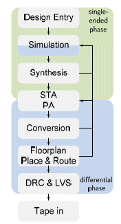
Fig. 1. Phases of the ECL Design Flow.
These libraries contain the timing data for each internal timing path, area factor, maximal load capacitance, additional timing constraints (setup time, hold time) and the boolean function of each singleended ECL cell. Therefor, an optimization strategy for area, timing specification and power dissipation is possible.
As a result of this gate-level synthesis, a singleended Verilog netlist and the related timing data is exported. Static timing and dynamic power analysis can be done easily afterwards to estimate the performance of the circuit.
Since the Verilog netlist contains single-ended ECL gates that do not exist at layout level, an additional development phase is introduced within the general digital CMOS Design Flow. In this differential phase, a netlist converter analyzes the synthesized single-ended netlist and replaces single-ended gates by fully differential ECL gates. Essential differential logic wires, analog supply cells and additional supply nets, i.e. control voltages for the current sources of the ECL gates, are added to the design. The outcome is a completely differential Verilog netlist, which can now be imported in the backend tool. Differential Verilog simulation libraries are provided to enable differential timing simulations and verification. This type of library includes a differential behavioral model of each ECL logic gate as well as essential supply cells. As a consequence, a static timing analysis (STA) and a differential timing simulation of the converted differential netlist are mandatory. This is important due to increased propagation delay of a differential ECL gate that can be occurred by additional single-ended fanout of both single-ended outputs at the conversion step. In order to perform this analysis, the differential synthesis/timing libraries can be used to analyze the timing behavior and to export the resulting timing data.
The differential Verilog netlist can be simulated with timing data in a HDL Simulator using the linked differential Verilog Simulation Libraries. Therefor, possible re-synthesis and redesign have to be taken into account in an early state while developing an ECL design using this flow. The layout of a differential ECL design is done in the next step and quite similar to the standard digital CMOS Design Flow. The backend tool reads in the differential Verilog netlist and its design constraints.
Furthermore, the differential timing library and the technology file are linked to the place and route tool. After placing the gates, differential nets can be routed. Additional constraints, such as netmatch or the diffpair attribute should be specified for each differential net pair to achieve a better RC routing match of the differential pair.
A Clock Tree Synthesis (CTS) in a fully differential ECL design is not yet supported in this methodology. Therefor, the essential constraints have to be set at synthesis level. The final layout can be exported as a differential Verilog netlist, its related timing data in Standard Delay Format (SDF) and the design as GDSII or Data Exchange Format (DEF). Consequently, a final differential Post Layout Simulation can be easily done as illustrated in Figure 1. After fixing possible DRC errors, a LVS can be performed and the differential ECL design can go into fabrication.
A. ECL GATES
In order to make the synthesis of differential logic possible using standard development tools, differential logic has to be made readable for RTL Compilers. Therefor, the differential logical functionality of each ECL gate is modeled in a simple CMOS-like single-ended behavior.
Crossing a differential input or output pair of an ECL gate corresponds to logic function of invertor. For instance: universal differential two level ECL gate unidiff has an OR functionality as a result of the voltage difference of Qp and Qn. The NOR functionality is easily derived by crossing the differential outputs; the function is inverted.

Tab. 1.Functionality depending on crossed inputs pairs.
Both logic functionalities are expressed by separated single-ended output pins for each ECL gate, whereas the basic differential logic function is given by the voltage difference of Qp and Qn and represented by Q_out, and Q_not vice versa. Crossing the differential input pairs and using De Morgan’s laws results in the following logical functionalities related to the output pin Q_out as shown in Table 1 and Figure 2.
This modeling of functionality is done for each differential input pair of an ECL gate, and described as a single-ended logic cell in the synthesis library.
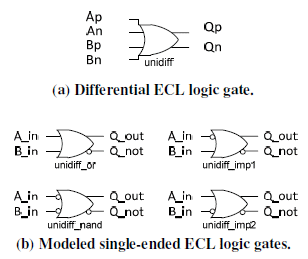
Fig. 2. Modeling differential logic in single-ended functionalities.
B. LIBRARIES
The resulting behavioral model of each singleended gate is added to the Verilog simulation library to provide a gate level simulation following the HDL implementation and/or synthesis. In order to get necessary timing information for the synthesis libraries (single-ended), all schematics of the ECL standard cells are simulated in parameterized test benches with SpectreMDL. Essential information, like propagation delay depending on different capacitive loads, drain current of the current source NMOS transistor and slope were extracted and reordered in a spreadsheet format. The exported raw data is parsed using standard Unix tools such as sed and awk to translate into the LibertyTM Format. The area and drive capability are added afterwards to the library.
However, the content of the differential timing libraries and their corresponding single-ended libraries is nearly the same, except the timing paths are adapted and the function attribute of the output pins in the differential versions is missing. Therefor, these libraries can only be used for static timing analysis and power analysis.
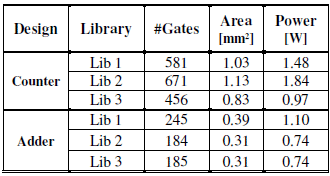
A gate-level optimization during synthesis without a specified function attribute in a timing library is not possible. During development of this digital design flow, different approaches of modeling ECL gates as synthesizable standard cells are carried out. Table 2 shows a comparison of three ECL synthesis library realizations. The first ECL library Lib 1 contains only single-ended ECL cells with singleended input and complementary outputs (see unidiff_or gate in Figure 2).
This library is a subset of Lib 3. No crossed input versions are implemented, but all functions can be derived by concatenating appropriate gates. Second approach, Lib 2, contains differential ECL gates as several types of single-ended gates with crossed differential inputs. Negating outputs are not part of this library.
This is quite similar to most CMOS standard cell libraries and better readable for standard synthesis tool if gates are more complex. Our proposed methodology is modeled as illustrated in Figure 2 and represented by ECL library Lib 3. It uses the minimal area and power effort to realize the desired behavior of 32-Bit counter and 32-Bit adder with given equal timing and power constraints as one can see in the following table.
Tab. 2. Synthesis results of different modeling approaches.
IV. DIFFERENTIAL CONVERSION
The synthesized single-ended Verilog netlist contains single-ended inputs, single-ended outputs and alternative cell names used for mapping the technology, as shown in Figure 2 (a).
At this time, the connections of necessary supply wires for power, current sources and control voltages are not taken into account. Therefor, a conversion step is introduced to generate a differential Verilog netlist.
The synthesized single-ended Verilog netlist is read in into the netlist converter. In a first converter step, all single-ended cell names are replaced by differential ECL cell names. The pin name of every pin indicates the signal category, i.e. single-ended reset, logical differential or logical single-ended. In a second step, a complementary pin is added to the cell for every pin of the differential pair category. The wire connections of the new differential pair are done simultaneously. Under certain conditions, the fanout load of a differential output pair is increased after the conversion, as shown in Figure 3 and Figure 4. This occurs, if both output pins (Q) of a single-ended ECL cell are connected to further input pins. As a consequence of the conversion, the differential fanout load is determined by the sum of the single output fanout of these pins. This results in larger propagation delay which has to be taken into account while constraining the design.
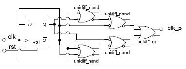
Fig. 3. Synthesized single-ended ECL circuit.
In the last step, essential biasing and initialization cells are added to the differential netlist. Furthermore, the resulting top-level pins are created. As a result, this netlist can be simulated and is prepared for backend tools to start the layout development.

Fig. 4. Converted differential ECL circuit.
V. DESIGN EXAMPLES
The proposed digital design flow was already utilized for some applications: The first synthesized ECL design was published in 2008 by H. Gustat et al. in [9]. This ECL FIFO consists of two Mueller pipelines with a capacity of 4x8 bit each and works at 3 GHz with a power consumption of 1.05W. The second synthesized ECL design is used as clock divider for a local oscillator in satellite communications as presented by F. Herzel et al. in [10]. Furthermore, a LVDS interface (CMOS to ECL and ECL to LVDS) was implemented as an output for a digitally controlled oscillator of an all-digital phaselocked loop as published in [11].
The layout of the most recent design, a 1:16/16:1 CMOS/ECL (de-)serializer, is shown in Figure 5.
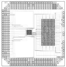
Fig. 5. Layout of the serializer.
This chip is divided into a 4:16/16:4 CMOS (de-) serializer and a 1:4/4:1 ECL (de-)serializer. It uses fast CMOS to ECL and ECL to CMOS converters for interconnection between both logic families. The static power consumption of the ECL component is about 0.5W, whereas the maximum frequency of more than 7 GHz was simulated with a power supply of 2.5V at room temperature. In contrast to ECL, the maximal working frequency of the CMOS part is about 250MHz with a related power consumption of 3.6mW.
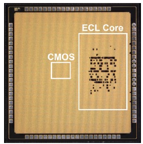
Fig. 6. Chip photo of the fabricated serializer.
The large HBT devices used in ECL standard cells result in a dimension of 1.0mm x 1.6mm for the differential core. Whereas, the core area of the CMOS core is 0.37mm x 0.3mm. The standard cell height ratio between CMOS to ECL is 1:7. Figure 6 shows the fabricated chip of the mixed signal serializer.
VI. CONCLUSION
In this paper a digital design flow is presented in order to develop differential ECL designs with utilization of standard CAD tools. Starting from the HDL description at Design Entry level, the synthesized netlist is translated by a Verilog netlist converter. As a result, a fully differential Verilog netlist is ready for differential static timing analysis, simulation and early verifications.
In order to ensure a sufficient logical mapping at synthesis level, a set of single-ended cells is modeled for each differential ECL gate. Additionally, most of the cells are available in different speed classes that leads to a compromise of power and high performance designs. As a consequence, the number of cells of single-ended libraries grows fast with each new added cell. Moreover, the usage of differential netlists as an input for backend tools doesn’t support boolean optimization at physical level due to missing function attribute of differential cells in LibertyTM format. Especially, a clock tree synthesis is not supported yet.
However, this flow is useful for differential, high performance components in mixed signal designs. The whole design can be designed in one shot with commonly used synthesis and backend design tools. The introduced conversion step, before the layout phase, makes it possible to perform differential analysis directly after synthesis. This saves development time, if more design iterations are necessary. Furthermore, all used backend libraries have differential cell layouts: no single-ended layouts with thick pin area or thick metal connections are used. Additionally, there is no need to modify post layout data using post processing scripts.
It is planned to extend this flow further and correct the mentioned deficiencies such as Clock Tree Synthesis. After this flow is improved, the design-inone- shot of more complex, differential designs will be enabled.
VII. ACKNOWLEDGEMENT
The authors want to thank the colleagues from IHP Hans Gustat, Frank Herzel and Ulrich Jagdhold as well as Gerald Kell and Daniel Schulz from Brandenburg University of Applied Sciences for their contribution.
REFERENCES
[1] N. A, “Early Transistor History at IBM,” web, semiconductormuseum.com.
[2] D. Lewine, J. Guyer, B. Baxter, and C. Moriondo, “An ECL implementation of the Motorola 88000,” in COMPCON Spring ’89. Thirty-Fourth IEEE Computer Society International Conference: Intellectual Leverage, Digest of Papers., feb-3 1989, pp. 27 –31.
[3] E. W. Brown, A. Agrawal, T. Creary, M. F. Klein, D. Murata, and J. Petolino, “Implementing Sparc in ECL,” IEEE Micro, vol. 10, pp. 10–22, 1990.
[4] P. Belemjian, O. Erdogan, R. Kraft, and J. McDonald, “SiGe HBT Microprocessor Core Test Vehicle,” Proceedings of the IEEE, vol. 93, no. 9, pp. 1669 –1678, 2005.
[5] V. Morgan and D. Gregory, “An ECL logic synthesis system,” Proceedings of the 28th ACM/IEEE Design Automation Conference, pp. 106 –111, 1991.
[6] Synopsys Inc., S. 0. Documentation, Design Compiler, Library Compiler and Data Preparation, 2007.
[7] S. Badel, I. Hatirnaz, Y. Leblebici, and E. Brauer, “Via-programmable structured ASIC fabric based on MCML cells: Design flow and implementation,” in Circuits and Systems, 2006. MWSCAS ’06. 49th IEEE International Midwest Symposium on, vol. 1, Aug. 2006, pp. 85 –88.
[8] S. Badel, E. Guleyupoglu, O. Inac, A. Martinez, P. Vietti, F. Gurkaynak, and Y. Leblebici, “A Generic Standard Cell Design Methodology for Differential Circuit Styles,” in Design, Automation and Test in Europe, 2008. DATE ’08, 2008 , pp. 843 –848.
[9] H. Gustat, U. Jagdhold, F. Winkler, M. Appel, and G. Kell, “Differential ECL/CML Synthesis for SiGe BiCMOS,” in Compound Semiconductor Integrated Circuits Symposium, 2008. CSIC ’08. IEEE, 2008, pp. 1 –4.
[10] F. Herzel, S. Osmany, K. Hu, K. Schmalz, U. Jagdhold, J. Scheytt, O. Schrape, W. Winkler, R. Follmann, D. Köther, T. Kohl, O. Kersten, T. Podrebersek, H.-V. Heyer, and F. Winkler, “An integrated 8-12GHz fractional-N frequency synthesizer in SiGe BiCMOS for satellite communications,” Analog Integrated Circuits and Signal Processing, vol. 65, pp. 21–32, 2010, 10.1007/s10470-010- 9454-z. [Online]. Available: http://dx.doi.org/10.1007/s10470-010-9454-z
[11] O. Schrape, F. Winkler, S. Zeidler, U. Jagdhold, and E. Grass, “An All-Digital Phase- Locked Loop with High Resolution for Local On- Chip Clock Synthesis,” PATMOS, 2010.
Related Semiconductor IP
- NPU IP Core for Mobile
- NPU IP Core for Edge
- Specialized Video Processing NPU IP
- HYPERBUS™ Memory Controller
- AV1 Video Encoder IP
Related White Papers
- Multi-Channel Multi-Rate (MCMR) Forward Error Correction (FEC) - IP for High Speed Networking Applications
- Serial Peripheral Interface. SPI, these three letters denote everything you asked for
- Shift Left for More Efficient Block Design and Chip Integration
- Linearity Analysis of Source-Degenerated Differential Pairs for Wireline Applications
Latest White Papers
- Ramping Up Open-Source RISC-V Cores: Assessing the Energy Efficiency of Superscalar, Out-of-Order Execution
- Transition Fixes in 3nm Multi-Voltage SoC Design
- CXL Topology-Aware and Expander-Driven Prefetching: Unlocking SSD Performance
- Breaking the Memory Bandwidth Boundary. GDDR7 IP Design Challenges & Solutions
- Automating NoC Design to Tackle Rising SoC Complexity