IP Exchange Through Handoff for Easy System-On-Chip Design
Rahul KHETERPAL, Atul NAURIYAL, Vivek SINHA (STMicroelectronics)
Abstract:
Over the past ten years, as integrated circuits became increasingly complex and expensive, the industry began to embrace new design, reuse and optimisation methodologies for doing System-on-Chip (SoC) design.
Design of such SoCs typically relies on multi-team, multi-site cooperation and data exchange. Intellectual Property (IP) Reuse is one of the keys for SoC design efficiency improvement; so alongside designing IPs, it is very important to be able to put them to appropriate use in future designs. This has also been extended to SoC subsystem exchange.
This paper provides insight into a novel solution used to build SoCs targeting increased productivity in a complex environment. It describes the IP exchange and checking infrastructure deployed in a live design environment to ensure a well-timed and transparent transference of the sub-systems from the handoff to the implementation team.
The solution targets an automation-capability which plays a vital role in extracting from the design repositories the relevant IP files and automatically performs the environment creation necessary for executing design handoff checks in-situ. This paper describes a design-automation method which emphasises on eliminating human intervention each time a design is to be re-introduced, ensures easy top-level absorption, parallel debugging and group handling of several IPs, thus guaranteeing schedule savings.
The first section will present an introductory overview of the handoff process and the recommended method will follow in detail later. The subsequent sections depict the working model as well the benefits of the approach. Necessary observations and statistics to justify the benefits are also provided. Further scope of extension is also addressed.
INTRODUCTION
A designer’s productivity is being continuously out-paced by the size and complexity involved in designing of electronic systems and devices, and there is a need to regularly seek new solutions in design methodology productivity and tools.
Deep submicron designs rely on increasingly sophisticated design tools and the reuse of pre-existing Intellectual Property (IP). The success or failure of System-on-Chip (SoC) designs rests evenly on quality of the IP and the ability of the tools that integrate them, and the skill of the designers implementing it.
A number of design methodologies have been created and implemented to help improve competencies at handling larger designs. The wide adoption of design reuse and exchange of entire functional blocks (IPs) has led to major gains in SoC design efficacy.
Verification methods applied on the IP design during SoC integration phase emphasize on the correctness of IP cores and multi-IP integration so as to implement the application functionality.
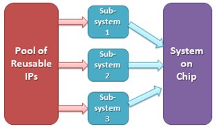
Figure 1: SoC Design Process
IP-Reuse methodology
`IP re-use` was introduced to cope with very large and complex designs. It principally involves re-using of functional units/IPs with well-defined functionality with the purpose of including exactly the same IP on multiple SoCs. There-by speeding up SoC design.
IP-Exchange methodology
IP re-use is the vital link for quick, easy and superior SoC integration; hence having a model to manage exchange of IPs is more than just a quality prerequisite. `IP Exchange` refers to the whole sequential flow wherein SoC team requests for an IP, the IP team develops/designs it, and eventually delivers that IP to SoC team for chip integration. This process is complex and by construction involves many parties (often across geographies). It also involves many steps in both directions IP to SoC and SoC to IP. There are generally few processes available to guide and control this activity.
Proposed methodology
This paper focuses on the dynamics and methodology related to internal IP exchange, and puts in place a simple and efficient process model. The model discussed here has a minimal set of steps that ensures speedy, clear and reliable transactions during the handoff process, as part of IP exchange.
BUSINESS MOTIVATION
Three key drivers of our approach are: Time-to-market, Development cost of design, and the largely manual process of Handoff. For silicon suppliers the costs of high end complex SoC- the cost of masks and fabrication has increased exponentially.
To tackle these challenges early-on in Design Flow, designers are turning to new methodologies i.e. SoC integration platform, IP re-use and exchange, and increased optimisation at every possible step of Design Cycle from specification creation till GDSII Tape-out.
The proposed IP exchange model plays a crucial role in achieving faster time to market, by automating IP infrastructure and the incoming quality assurance steps. This approach also tends to increase reliability and quality, by reducing manual steps, and thereby lessening any human errors.
THE HANDOFF PROCESS
Handoff involves catching issues early concerning design quality, which if not caught will appear in later implementation stage.
Functional precision of the IPs being integrated has to be safeguarded before the SoC integration phase.
Efficiently synthesizing a chip requires managing a large amount of data along with its constraints, dependencies and interrelationships. Synthesis becomes progressively tough as block size increases. Therefore, a "hand-off" of the synthesized Netlist occurs several times, from the logical/system designers to the physical implementation designers during design cycle, as shown in the figure below.
In a traditional ASIC flow, numerous iterations between the front-end team and the back-end team take place, to implement the Netlist on layout, which meets the sign-off criteria and can be taped out. With increasing complexity of designs at lower technology nodes, this back and forth cycle gets increasingly schedule-expensive.
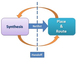
Figure 2: The Netlist Handoff Process
The illustration drawn below indicates the cycle of iterations between the teams and the time spent in achieving the desired result. To converge to the anticipated Netlist, in our design teams the front-end used to take 3 weeks of time by following the traditional manual handoff flow.
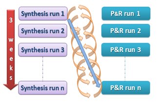
Figure 3: Iterative Process in a handoff flow : TRADITIONAL APPROACH
Hence, what is required is a Netlist handoff solution that delivers a timely and reliable design while addressing timing analysis, Linting & clock domain crossing checks, and checking quality of constraints.
RECOMMENDED APPROACH
In a perfect world, a single-pass of synthesis could be followed by single-pass of handoff which could be followed by a single-pass of Place and Route, leading to a GDSII creation. Realistically, with several variables existing, and late functional changes being routinely accommodated, such a one pass flow is not feasible.
This implies multi-pass handoff runs. Since handoff is largely a manual process, an automated approach is recommended for a sustainable and promising delivery in speedy time. This is based on a non-Design-specific platform and can be easily replicated in any SoC design project.
The driving forces and outcomes of this approach for the handoff process are visualised below:

Figure 4: Thematic Model of the Recommended Approach
AIM
The purpose of the model shown above is to smoothen and accelerate the handoff process in order to facilitate IP exchange. IP blocks have to go through various stages during design maturity, viz. RTL, post Built-in-Self-Test inclusion, post synthesis, post DFT inclusion and prior to and post physical implementation, thereby increasing design files with several corrected releases.
The technique discussed here aims to keep manual efforts of the designer in organising and setting-up IPs after each design maturity stage to perform major Front-End level checks to bare minimum. In this way, the designer can spend quality time on debug and analysis, of the various checks. The same practise is extended to the integration phase of the IPs onto the SoC level, hence making the design integration easy and reliable through clean handoff.
OPERATIONAL MODEL
As outlined in the aim section, this approach does the necessary preparation for handling IP blocks to perform handoff checks which was cumbersome earlier. The primary inputs are: synthesized netlist, design constraints and technology libraries (liberty file).
The automation builds the mandatory infrastructure for the checks, in the format as supported by the EDA tools. The inputs are managed along with the customisations required for the flow to run systematically. All this is processed in parallel and the checks viz. lint checks, clock checks, constraints optimization, clock domain crossings and SoC integration checks are also performed across all blocks in the same fashion.
Some salient features of this methodology are discussed in the later section. A demonstrative comparison is also presented in the forthcoming section that showcases features and benefits of the approach. This automated method can be visualised in the figure shown below:
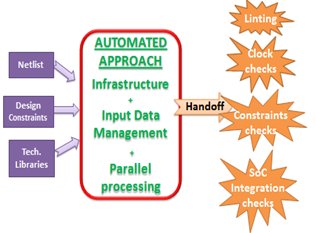
Figure 5: Working Model of the Recommended Approach
Main Features and Key Benefits of the proposed solution are:
1. Infrastructure management: It organises and structures the environment over which the EDA tools can be set-up.
- Customisations of IP design files from design repositories are correctly done based on the syntax understood by the EDA on these files. Hence, the execution is feasible involving zero manual rectifications.
- The selection of checks per IP block is maintained through a comma delimited file (.csv) which is easy to write and understand.
2. Input Data management: All the inputs viz. netlists, block constraints and the libraries are fetched with their latest versions in every release.
- Data linking is robust and seamless, thus making the subsequent processes easy and less time consuming.
- Libraries are also precompiled for the EDA flows that require them, while automation maintains the library versions as well.
- For the desired checks, the appropriate set of rules is picked along with the aligned EDA tool per design block.
3. Parallel processing: This automation is capable of handling hundreds of runs of the checks for all the IP blocks in parallel.
- This is achieved by the efficient use of Load Sharing Facilities in the design houses.
4. Accuracy: With manual efforts bare to minimum, the model promises high degree of accuracy and near to zero faults.
- Applying filters/waivers to messages for easy suppression during the next design-check run is handled seamlessly in the background.
5. Debug insight: The ability to analyze the inside of a design, i.e. being able to access signals, registers and the state of the hardware/software design, is considered crucial and the intent of this approach matches seamlessly.
i. This method supports incremental reporting of violations between versions of the design netlist across design stages.
6. Cost savings: Reduces cost and the time to reach top-level integration, eventually improving the time-to-market. Human resource savings is also achieved, as one person is able to run 30 IP blocks, which required multiple resources with manual processes earlier.
Crucial checks done on the design during handoff are:
1. Lint checks: Extensive set of syntax and lint checks are performed. These include checks related to synthesis, functionality, DFT and physical implementation issues.
2. Constraints checks: The design constraints are checked based on their consistency with the design so as to define the correct design intent.
3. Clock Domain Crossing (CDC) checks: Checks related to the missing synchronizers between asynchronous clock domains.
4. SoC integration checks: Connectivity checks between various IP blocks with respect to Top.
An illustration can be drawn relative to the one shown previously, on the traditional handoff flow, to depict the recommended/improved flow:
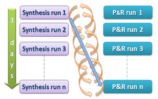
Figure 6: Iterative Process in a handoff flow: RECOMMENDED APPROACH
It is evident from figure 6, that the front-end team took 3 days effectively by using the recommended approach instead of 3 weeks as earlier (figure 1).
Thereby, the approach is achieving a 7X gain in delivery time.
DEPLOYMENT ON LIVE PROJECT: RESULTS
This automated approach was used on a live SoC design having size of 500mm2 with around 30 IP blocks. Table given below shows a quantitative comparison between the traditional and the recommended approach in terms of the designer’s time in executing Handoff on these 30 blocks.
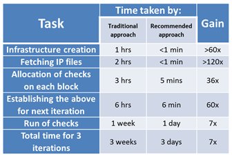
Table 1: Quantitative comparison between the traditional and the recommended approaches
Pictorial view, of the above statistics, shows efficiency of the recommended approach:
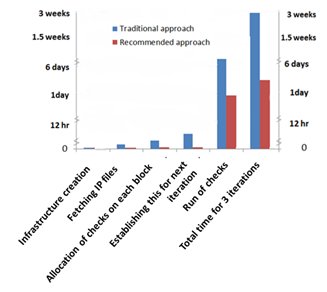
Figure 7: Comparison of time taken by the two approaches
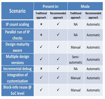
Table 2: Qualitative comparison between the traditional and the recommended approaches
SUGGESTED EXTENSIONS
Next extension of this approach can involve utilizing physical-aware checking/analysis techniques at IP or subsystem level earlier-on in the flow (e.g., during the handoff process). The resulting netlist would then become implementation-friendly with respect to physical constraints, floor plan, congestion and timing needs as well. This implies a new paradigm of ‘physical effects anticipation’ at RTL or early-netlist level, to further improve design quality and schedule-predictability.
CONCLUSION
Cost and schedule savings were realized by developing & deploying an approach as described above, to enable exchange and SoC integration of IPs across design teams. The paper has captured some of the viable components of handoff infrastructure as part of a methodology which aims at improving the difficult process of Design netlist handoff. It has presented the gains realized through this method with recent live project QoR figures.
ACKNOWLEDGEMENT
The authors wish to thank the following people who have contributed to this paper and to the methodology:
1. Rangarajan RAMANUJAM, STMicroelectronics
2. Sakshi GUPTA, STMicroelectronics
3. Nirmal PREGASSAME, STMicroelectronics
REFERENCES
1. SpyGlass® 5.1 Atrenta Console User Guide
2. R.Saleh, S. Wilton, S. Mirabbasi, A. Hu and others, “System-on-Chip: Reuse and Integration”;
Proceedings of the IEEE, 2006 (Vol:94, Issue: 6)
3. W. Savage, J. Chilton, R. Camposano, “IP Reuse in the System on a Chip Era”; System Synthesis, 2000
4. Rosamaria Balestri, “IP Exchange Procedure”; IP-SOC, 2004
5. M. Strik, A. Gonier, P. Williams, “Subsystem Exchange in a Concurrent Design Process Environment”; DATE, 2008
6. Invaluable discussions with SoC designers of STMicroelectronics
Related Semiconductor IP
- PDM Receiver/PDM-to-PCM Converter
- Voltage and Temperature Sensor with integrated ADC - GlobalFoundries® 22FDX®
- 8MHz / 40MHz Pierce Oscillator - X-FAB XT018-0.18µm
- UCIe RX Interface
- Very Low Latency BCH Codec
Related Articles
- Integrating VESA DSC and MIPI DSI in a System-on-Chip (SoC): Addressing Design Challenges and Leveraging Arasan IP Portfolio
- System-on-chip (SoC) design is all about IP management
- Design and Implementation of Test Infrastructure for Higher Parallel Wafer Level Testing of System-on-Chip
- Formal-based methodology cuts digital design IP verification time
Latest Articles
- A Scalable Open-Source QEC System with Sub-Microsecond Decoding-Feedback Latency
- SNAP-V: A RISC-V SoC with Configurable Neuromorphic Acceleration for Small-Scale Spiking Neural Networks
- An FPGA Implementation of Displacement Vector Search for Intra Pattern Copy in JPEG XS
- A Persistent-State Dataflow Accelerator for Memory-Bound Linear Attention Decode on FPGA
- VMXDOTP: A RISC-V Vector ISA Extension for Efficient Microscaling (MX) Format Acceleration