Improving Design Timing and Simplicity for Lower Cost and High Performance Multistandard Audio Decoder STA012
Sam BORDBAR, Synopsys, Inc.
Sal TIRALONGO, Synopsys, Inc.
Milan ITALY
Abstract
The complexity of today's System On Chip (SoC) designs requires a faster and simpler flow and methodology for new SoC design projects.
So, to get more SoCs to market faster-and less expensively-STMicroelectronics Audio Division (Audio & Automotive Group) combined forces with Synopsys® Professional Services to conceive a new flow and methodology for Audio Decoder.
The collaboration will provide ST SoC design teams with a low-cost solution, by extending Synopsys' AMBA DesignWare to support STMicroelectronics' STA012.
The STA012 is a highly integrated multi-standard audio codec with embedded CD-ROM decoding & MMC/SD reading/writing capabilities. The user can download music and also update the STA012 audio algorithms via the FLASH/SDRAM interface available on the device or via the CDROM interface; during play back the data stored into the external storage media are fetched and processed by the audio decoder.
To fetch instruction and read/write data to the external memories an AMBA DesignWare memory controller (DW_memctl) has been used.
The DW_memctl MacroCell is a memory controller can be configured and synthesize in order to control Synchronous DRAMs - SDR-SDRAM, Mobile-SDRAM, DDR-SDRAM, and the Micron SyncFlash - as well as Static memories - SRAMs, FLASHes, and ROMs.
The integrators of this IP can simply loads this coreKit and configure it using the friendly graphical interface provided by Synopsys' coreConsultant, to obtain an RTL view and/or a gate level netlist of the configured MacroCell.
The idea is to allow the designer to rapidly assemble, synthesize and verify an SoC through a new methodology which uses coreKits in the system, together with the target library and generate a configured and connected RTL, together with the most appropriate synthesis strategy. All of this is part of an overall SoC flow that includes interactions with other tools such as: Synopsys' Physical Compiler, PrimeTime, and more.
As a result, STMicroelectronics is finding that even the most complex sub design requires less in-depth knowledge of the IP, and also reduces the support load for the IP developers. Usage of the Synopsys' DesignWare memory controller even decreases the silicon area by not including the unneeded and unused features.
Because STMicroelectronics has simplified the effort by using this methodology, the integrator can spend more time thinking about the system architecture, instead of solving implementation issues. The design that would take two months to implement can now be done in two weeks, and one that would take two weeks can now be done in two days.
Improving Design Timing and Simplicity for Lower Cost and High Performance Multistandard Audio Decoder STA012
1.0 Audio Decoder STA012
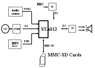
The STA012 is a highly integrated multi-standard audio decoder with embedded CD-ROM decoding capability.
It includes a 24-bit VLIW DSP specifically conceived to implement the encoding and decoding of complex digital audio formats and can be easily connected to most existing CD devices via a software configurable serial link. The user can download music via the External memory interface available on the device; during play back the data stored into the external storage media are fetched and processed by the audio decoder. A bypass mode allows the use of the device also as an audio processor for volume and tone controls. Unused parts of the device can be shut down to minimize power consumption.
The program code can be executed from the internal ROM or the external memory.
1.2 Different Systems
1.2.1 ROM Based System
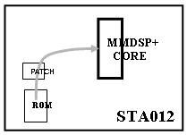
The code is stored in the internal ROM; the system can be considered low cost because no external memory is needed but the code cannot be update.
The only feature available is to patch small piece of the code thanks to a patch memory.
1.2.2 Cache Based System
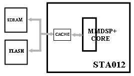
The code is stored into an external flash then can be easily modified without any impact on the system. If high performances are required it’s possible at the boot to move the code from the flash to an sdram and then fetch the instruction from there.
The devices can decode/process data coming from five possible sources:
- CDDSP serial link: using this input interface, besides MP3 encoded data CD, it's possible to playback also standard Audio CD using the available volume and tone equalizer features of the device and allowing the use of only one D/A converter with no external analog switch.
- EMI interface: through this interface it's possible to download or store an audio bit stream from or to external memory
- SDI input interface: used to decode ADPCM streams.
- I2S input interface: this interface can be used either to encode an external audio source (with variable compression based on 4 different ADPCM algorithm) or to process an external audio source (tuner, for instance) through the DSP volume and tone controls: the BYPASS mode can avoid the use of additional D/A converters or post-processing units.
- MMC/SD serial links: there are two slots where it is possible to connect two cards at the same time.
- Port-0 accepts SD card in single-mode (1-bit Data Channel) or MM card.
- Port-1 accepts SD card in wide-mode (4-bit Data Channel) or MM card. Decoded audio data goes through a software volume control and a two-band equalizer blocks before feeding the output I2S interface.
- The basic functions of the device can be fully operated via the I2C bus.
1.3 Audio Decoder Engine
The audio decoder engine is designed to support several audio formats including:
- MPEG 2 layer 3 (MP3) decoder supporting:MPEG 1, MPEG 2 Audio
- Lower sampling frequencies syntax extension called MPEG 2.5
- MP3PRO decoder
- AAC stereo decoder
- WMA decoder
- MP3 encoder
- ADPCM encoder/decoder engine
1.4 System Architecture
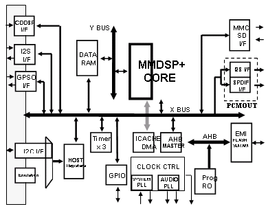
The system is based on a simple AMBA architecture. The MMDSP+ core is the master and on the AHB bus two peripherals are integrated: a ROM and a memory controller.
The MMDSP+ core is associated with data memories and a 2 level program cache. Some peripherals are also integrated into this Core: 3 timers, a Multimedia and Secure Digital Cards interface, a16 bit GPIOs interface, an I2C slave interface an AHB master interface associated with the internal cache memory.
The DSP core is a 24 bit Harvard, VLIW, load/store instruction set processor. The instructions are executed in one clock cycle.
The DSP supports different types and sizes of memory data (16/24 bits short data, 32/48 bits I data and 40/56 bits long data).
1.4.1 The MMDSP+ Instruction Cache
Two levels of cache are used to minimize the power consumption. The second level of cache (L2) is build around a tag RAM (4 standard RAMs) and a data RAM (standard RAM generator). This cache is a multiway associative cache. The first level of cache (L1) is used to decrease the number of accesses to the data RAM and Tag of the L2 cache, and thus the power dissipation. The replacement policy is Round-Robin and cache code lock is available.
1.4.2 The AHB Master Interface
For the MMDSP+ system, this AHB master interface can be used for both data access and program access.
Data access is a direct connection from X bus to AHB. Program access is intended to fill instruction cache lines. Data I/F and Program I/F are both connected to an AHB lite master. The conversion from AHB lite to full AHB is done with an ARM standard wrapper.
When both data access and program access are required at the same time, priority is given to data transfer.
With this interface the MMDSP+ has access to the whole AHB space
1.4.3 Program Interface
The AHB master program interface receives address and request from MMDSP+ Instruction cache, when a miss occur. The address provided by Instruction cache is a logical 32 bits address. A translation to AHB physical address is done by adding a base address stored in host registers and controlled by ARM system.
AHB transactions are always 4 words bursts.
1.4.4 Data Interface
The AHB lite master simply initiates AHB read or write access to the physical memory location addressed by X bus external access.
Two modes are available for this master behavior:
- Simple: each X bus transfer is converted to a single AHB transfer
- Pipelined: X bus write are registered in a FIFO, X bus read always initiate a 4 words burst to anticipate further X bus read in consecutives address.
In that mode, MMDSP word are considered as 24 bits data. A 24 bits word in MMDSP is located inside a 32 bits word of external memory.
1.4.6 Mode 16/16 bits
In that mode, MMDSP words are considered as 16 bits data. A 16 bits word in MMDSP is then located inside a 16 bits word of the external memory.
1.4.7 External Memory Interface
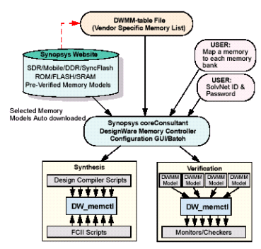
The DesignWare DW_memctl MacroCell, which is delivered as a coreConsultant coreKit, is a memory controller that controls SDR-SDRAM as well as Static memories – SRAMs, FLASHes.
The coreKit is an AHB slave in SOC designs and provides all the functionality for read/write transactions from AHB master to the interface memory devices.
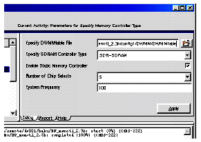
1.4.7.1 SDRAM Interface Features
As an SDRAM controller, the DW_memctl can support up to sixteen row address bits, fifteen column address bits, and four bank address bits. As a Static memory controller, the DW_memctl can support up to thirty-two address bits. The DW_memctl can support up to a maximum of eight different external memory banks. Only one set of timing registers control SDRAMs, so different SDRAM banks must have the same timings. If you are using the DW_memctl mode that controls a SDR/Mobile-SDRAM and a SyncFlash, two separate timing register sets are available for the SDRAM and SyncFlash. For Static memories, there are three different sets of timing registers.
SDRAM timing parameters – tRAS, tRCD, tRP, tWR, tWTR, tRCAR, tXSR, and tRC, – can be programmed to values supported by different SDRAM vendors Supports auto refresh with programmable refresh intervals, Supports self-refresh, Supports SDRAM power-down mode, Programmable immediate precharge or delayed precharge modes and Supports 1 to 16 (programmable) open banks for performance; pages can be non-contiguous – Least Recently Used (LRU) algorithm used during page miss replacements.
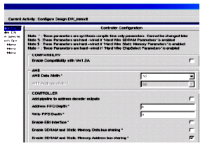
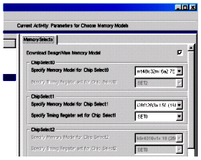
By using the Synopsys coreConsultant tool supplied with the DW_memctl MacroCell, we specified parameters based on our design specifications to describe the memory controller; coreConsultant then automatically configured, synthesized, and verified the components for our design environment and generated preverified DWMMs (Because we decided to use DesignWare Memory Models) and also automatically configured the DW_memctl core with the timing parameters for the those DWMM that we used.
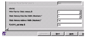
Supports asynchronous SRAMs, page-mode FLASHes and ROMs Supports up to three sets of timing registers Configurable address width of up to 23 bits Memory data width can be configured to 8, 16, and 32. Supports external “READY” handshake pin to interface non-SRAM-type device. Limited synchronous SRAM and FLASH interface support
Synchronous SRAM and FLASH frequency could be 1, 1/2, 1/3, 1/4, … of the AHB frequency.
Above we have seen a new way of implementing a complex IP, let's now take a deeper look at what it takes to develop and deliver an IP in this form.
2.0 IP challenge
The main principles in creating and delivering a reusable IP can be summarized as follows:
- Easily configurable to fit different applications
- Designed for use in multiple technologies
- Thorough commenting
- Well designed verification environments and suites
- Robust scripts
- Easy to use and friendly implementation interface
- Good documentation
The methodology described here addresses most of the above.
As an IP developer, you need to deliver an IP that can reliably be used by the integrator. The IP has to be easy to support and maintain, enabling long-term maintenance by capturing design knowledge. The business solution, which required direct support and a one-on-one knowledge transfer with every end user for an IP provider, would not be a viable one. The integration flow of an IP has to reduce all costs (not only the development cost but also synthesis, testing, integration in SoC, support and maintenance). In most cases, the end users want to customize the IP for specific applications. In order to achieve this effectively, few requirements have to be met, the creation of every stage of design, from specification to silicon has to be done with the understanding that it will be modified and reused in other projects by other design teams. It needs to use tools and processes that capture the design information in a consistent, easy to communicate form, and that make it easy to integrate modules into a design when the original designer is not available. Eventually, it should also force the integrator to go through specific tasks to synthesize and verify the core. The integration flow has to ensure quality of results, ease of use and tool support over multiple versions or licenses. The package has to provide all the necessary views and necessary tests across all possible parameters values. This core has to be not only easily configurable but also technology independent. Of course the protection of your IP is an important requirement for the developer.
Finally, this IP has to be easily integrated in an IP library and easy to be checked for reliability.
The innovation of core tools is to address all the previous needs: it has to provide industry leading tools that enable our users to create, package, deploy, integrate and assemble configurable soft IP.
The solution can be found in the new methodology offered by Synopsys’s suite of reuse tools.
3.0 Core tools methodology
3.1 coreBuilder, and coreConsultant
Within the coreBuilder suite of design reuse tools, the coreBuilder tool packages the developer’s knowledge of a design, along with the design’s source files, constraints and design information, configuration information, verification information, flow customization, and documentation, into a coreKit, which core integrators can apply across a spectrum of target technologies and applications.
CoreBuilder features a thorough, yet flexible activity flow that captures the core developer’s knowledge of a design. This process guides the core developer step by step through the configuration and packaging process, assuring that all the information the core integrator needs to implement the core as part of a larger application are entered.
The coreConsultant tool helps integrators configure, synthesize and integrate the core into chip-level applications. This tool leverages the core specific expertise packaged into the coreKit by guiding integrators through configuration, verification, and synthesis, enforcing parameter dependencies as necessary, and rejecting illegal configurations. Moreover, coreConsultant analyzes and summarizes the synthesis reports generated by Design Compiler or Physical Compiler, then presents the results to the integrator through a hierarchy of progressively more detailed data in text or html format.
3.2 Activity Based Flow
One of the main features of the design reuse tools described above is the concept of the activity-based flow. The core tools employ a sequential, ‘activity-based’ approach to packaging (coreBuilder), and integration/implementation (coreConsultant). In this sequential flow, certain activities are ‘dependent’ on others, which means that they can’t be begun until the dependent activity has been completed. For example, in coreConsultant you can’t begin any synthesis related activities until the configuration activity is complete. This approach provides maximum flexibility, while still providing sufficient structure to ensure that all requisite activities get completed, and that proper sequences prevail.
3.3 Core Tools flows
The coreConsultant activity flow has a similar look and feel to the coreBuilder flow. However, coreConsultant guides the user through the process of selecting an implementation, given a number of implementation options. Therefore what in coreBuilder are ‘setup’ activities in coreConsultant become ‘execution’ activities. This guided flow makes core integration very straightforward.
Before beginning to use coreConsultant, it’s necessary to install the packaged core and create a new working area for core implementation. The packaged core is available as the coreKit produced by coreBuilder. Using the installation workspace as reference, one or more ‘integration workspaces’ can then be created.
At this point the integrator can specify the ‘actual’ target technology for its implementation, choose a core configuration which meets its requirements, based on the available configuration options.
Once the target technology has been selected, and the configuration options set, the integrator can proceed to the synthesis related activities. Pre-defined synthesis intent can be modified where necessary, check that the final intent is correct and complete and finally generate the scripts for DC or PC and synthesize the core.
Through the verification environment the core user can also configure and run a regression for the core, once the HDL configuration is complete.
3.4 Enhanced tools support
The complexity involved in designing a System-on-Chip not only requires designers with different skills, but also requires many diverse tools as well. Design teams need to use the best tools available. The coreConsultant enable a large array of tools and leverage Synopsys tools as Design Compiler, Physical Compiler, Power Compiler, and FPGA Compiler.
Expert scripts relative to these tools (taking advantage of the best practices for each version) are integral part of coreConsultant tool.
The IP developer can allow the use of any other tools by the possibility to write a coreConsultant plugin defining a new activity to be run by the core integrator.
3.5 Core Tools Customization
coreBuilder and coreConsultant support flow customization. Steps (activities) that already exist within default activity flow can be modified to perform extra work. Additionally, you may add new steps to the default flow (link to other tools). These customizations are described in plugins (tcl). They can have a general impact on all coreKit or be specific to one coreKit.
Through the development and usage of plugins a developer can provide interfaces to any tools tailored to a specific design flow.
4.0 Conclusions
In this paper Synopsys DesignWare Memory Controller implementation flow methodology based on the Core Tools developed by Synopsys has been introduced, pointing out its advantages compared to the traditional design flow.
It’s evident how the new flow makes the design of a complex system such as the DesignWare Memory Controller quite simple, thanks to the user friendly graphical interface available with CoreConsultant, and safe from errors due to the automation of a variety of tasks previously performed by hands. Also the generation of all the different work environments, that is functional verification, synthesis and timing analysis environments, is automatic and configuration dependent, so that all the environments are generated taking into account the selected architecture of the DesignWare Memory Controller.
It’s worth pointing out that this design methodology, developed around the DesignWare Memory Controller, can be used also for the implementation of different DesignWare IP and custom IP, so it shouldn’t be seen as something specific for a well-defined application, but rather as a generic philosophy to be applied to IP design.
5.0 Acknowledgements
At the end, we want to point out that the achievement of the results described in this paper has been possible thanks to the fructuous cooperation between the STMicroelectronics and the Synopsys Professional Services division, whose contribution to the development of the new flow has been fundamental to shorten the time and to increase the quality of the work.
6.0 References
Related Semiconductor IP
- NPU IP Core for Mobile
- NPU IP Core for Edge
- Specialized Video Processing NPU IP
- HYPERBUS™ Memory Controller
- AV1 Video Encoder IP
Related White Papers
- Design and Implementation of Test Infrastructure for Higher Parallel Wafer Level Testing of System-on-Chip
- Shift Left for More Efficient Block Design and Chip Integration
- Rising respins and need for re-evaluation of chip design strategies
- How silicon and circuit optimizations help FPGAs offer lower size, power and cost in video bridging applications
Latest White Papers
- Ramping Up Open-Source RISC-V Cores: Assessing the Energy Efficiency of Superscalar, Out-of-Order Execution
- Transition Fixes in 3nm Multi-Voltage SoC Design
- CXL Topology-Aware and Expander-Driven Prefetching: Unlocking SSD Performance
- Breaking the Memory Bandwidth Boundary. GDDR7 IP Design Challenges & Solutions
- Automating NoC Design to Tackle Rising SoC Complexity