How silicon and circuit optimizations help FPGAs offer lower size, power and cost in video bridging applications
By Danny Fisher, Director of International Marketing, GOWIN Semiconductor
FPGAs are at home in the world of multi-gigabit-per-second signal conversion and bridging.
In high-bandwidth telecoms, network and data center equipment, the FPGA is a mainstay of system designs, offering a valuable combination of high-speed SerDes capability, extensive logic resources, and programmability, giving designers the flexibility to modify features and functions without changing their board layout.
Indeed, FPGA manufacturers have a long track record of creating products which are well suited to the telecoms central office or the data center environment: very fast and large chips which provide hundreds of I/Os, huge bandwidth, and built-in standard interfaces. The fact that they are also expensive and power-hungry is a bearable trade-off for telecoms and network equipment manufacturers.
Increasingly, however, the need for multi-gigabit-per-second rates in signal bridging systems is extending from telecoms and network equipment into consumer and industrial devices. Here, too, the FPGA offers valuable benefits. But large, expensive, power-hungry ICs are a poor fit for sleek, battery-powered consumer devices in the ultra-competitive markets for products such as tablets, laptop computers, and augmented/virtual reality (AR/VR) headsets.
This new demand in consumer electronics is forcing FPGA manufacturers to rethink the architecture of their products in a bid to provide high-speed SerDes functionality at lower cost and low power.
Gamers lead the way
The change which has precipitated a new wave of competition in the low-cost FPGA market has been led by demand from gamers: tablets and laptop computers have become the latest devices in which users want to play games in 4K resolution and – for smooth rendition of fast motion – at high frame rates of up to 160 frames/s.
The requirement for high-speed video signal transmission to support 4K displays stretches the capability of the interfaces that have previously been used in consumer devices to shuttle data from the central system-on-chip (SoC) to a display. Older MIPI D-PHY interface technology is giving way to the newer MIPI C-PHY standard for the most demanding 4K display applications in tablets and laptop computers. The doubling of the data rate in the migration from D-PHY to C-PHY technology poses a demanding challenge for low-end FPGAs.
Following the lead of the latest gaming tablets and computers, other use cases are now also starting to demand increased bandwidth in the link between an SoC and one or more displays, or between image sensors and an SoC. Examples include:
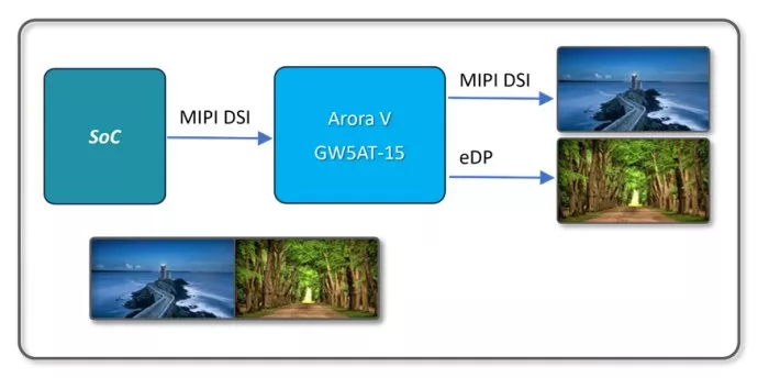
- Point-of-sale systems which split a single output from an SoC (typically in MIPI DSI format) to dual displays, one facing the consumer, one facing the sales counter. The FPGA typically converts the single DSI input to one DSI and one eDP output, with image processing to rescale the output and adjust the frame rate (see Figure 1)
- VR/AR headsets and goggles, splitting and converting a DisplayPort-over-USB Type-C® input from a host device such as a PC or smartphone to separate MIPI outputs to a left and right display in the headset
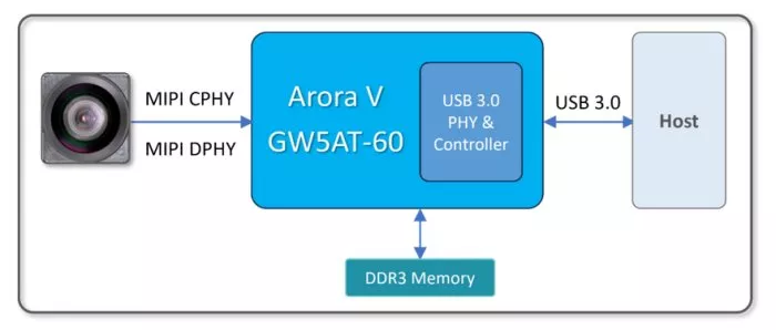
- Industrial machine vision systems, converting an image sensor’s MIPI D-PHY or C-PHY input to a high-speed USB 3.0 output to a host computer.

Fig. 1: using the GW5AT-15 FPGA, a single MIPI DSI video input from an external SoC can be converted to feed two displays requiring one MIPI output and one eDP output
Higher-speed SerDes at lower power and cost
In all these use cases, an FPGA can provide the raw SerDes throughput for one or multiple display screens or image sensors, while enabling changes in the input or output specifications to be made just by changing the VHDL or Verilog programming of the device. The question the consumer and industrial markets are asking is, how far can power consumption, size and cost be reduced while providing the high SerDes bandwidth these applications require?
GOWIN has provided a new answer to the question by combining application-specific optimizations at both the silicon and circuit design level in a way that no low-density FPGA has ever before attempted.
In silicon, scaling provides PPAC benefits (power, performance, area and cost) for low-end FPGAs as much as for other semiconductors. In the past, however, low-density FPGAs have tended not to take advantage of more advanced process nodes – FGPA manufacturers have preferred to extend the life of IP developed for legacy processes.
But high-speed video bridging places extreme demands on the FPGA. That is why for its Arora® V products, GOWIN shifted production from the 55nm process used in its Arora II products to TSMC’s ultra-low power 22nm process.
Use of this process has enabled GOWIN to gain performance, power and cost benefits in low-density Arora V products such as the GW5AT-15, available in a compact 4.9mm x 5.3mm WLCSP package. Despite its small size, this FPGA combines various hard-core SerDes transceivers offering maximum SerDes throughput of 12.5Gbps, together with 15,120 logic elements alongside high-speed memory resources including:
- 118kb of shadow SRAM
- 630kb of block SRAM (BSRAM) arranged as 35 x 18kb
- Optional 64Mb (in MG132P package) or 128Mb (in CM90P package) of pseudo SRAM (pSRAM)
- Optional 8Mb of NOR Flash
By limiting the programmable logic provision to 15,120 logic elements, GOWIN can produce a smaller die at a lower unit cost, while providing sufficient digital capability to perform important image processing functions such as frame scaling and frame rate adaptation.
The application-specific circuit design optimizations in the Arora V family provide the higher SerDes throughput required for instance by the gamers viewing 4K content at 160 frames/s on a tablet. For instance, the GW5AT-15 features hardcore implementations of important SerDes interfaces:
- Three-lane MIPI C-PHY (5.7Gbps/lane)
- Four-lane MIPI D-PHY (2.5Gbps/lane)
- x4 PCIe 2.0
Alongside these circuit features, the GW5AT-15 includes various built-in softcore interfaces suitable for video bridging applications: a USB 2.0 PHY, USB 3.0 PHY, PCIe 3.0, and up to four lanes of 12.5Gbps/lane SerDes suitable for DisplayPort, eDP, SLVS-EC, LVDS and other types of video traffic.
These capabilities are what is required for the gaming tablet rendering 4K video at a high frame rate, converting a typical SoC’s MIPI output to a tablet display’s eDP input (see Figure 2).

Fig. 2: conversion of video data from MIPI to eDP format in a gaming tablet requires high SerDes throughput
The implementation of fast video bridging and image processing is as important when interfacing to a camera as when rendering video on a display. In industrial machine vision systems, for instance, a GOWIN GW5AT-15 or -60 can connect to a camera’s MIPI D-PHY or C-PHY interface and bridge the video to a host PC’s high-speed USB Type-C interface (see Figure 3). The FPGA’s softcore USB 3.0 PHY and USB 3.0 controller enables a single-chip implementation that can interface directly to the host controller without an external USB 3.0 PHY.
This solution has an extremely small footprint which can be integrated into the camera enclosure.
The GW5AT-60, which offers 59,950 logic elements, provides sufficient resources to support image preprocessing and machine vision-related algorithms. It also provides high-speed four-channel SerDes transceivers, hardcore MIPI C-PHY and D-PHY interfaces, and softcore LVDS interfaces to support a wide variety of sensors.

Fig. 3: in an industrial machine vision system, use of an Arora V FPGA enables the USB 3.0 interface to a host PC to be integrated into the camera enclosure
A new direction for the low-density FPGA
The optimization of an FPGA product for video bridging and image processing applications points this segment of the low-density FPGA market in a new direction: in pursuit of greater size, power and cost reduction, FPGA products are evolving to include more application-specific SerDes functionality hard-wired into small devices.
And where previously FPGAs achieved low cost by maintaining older, legacy silicon fabrication processes, a new generation of low-density FPGAs are using advanced processes to provide the valuable advantages of low power and small footprint while reducing cost by limiting the provision of logic elements that are not required in the target applications.
This brings the FPGA to center stage in the consumer device market, enabling a new generation of devices to benefit from improved display and camera performance without sacrificing battery power or competitive cost.
Related Semiconductor IP
- NPU IP Core for Mobile
- NPU IP Core for Edge
- Specialized Video Processing NPU IP
- HYPERBUS™ Memory Controller
- AV1 Video Encoder IP
Related White Papers
- SoC goal staying alive: lowest cost, smallest size
- Improving Design Timing and Simplicity for Lower Cost and High Performance Multistandard Audio Decoder STA012
- How to Reduce Code Size (and Memory Cost) Without Sacrificing Performance
- How to lower the cost of PCI Express adoption by using FPGAs
Latest White Papers
- Transition Fixes in 3nm Multi-Voltage SoC Design
- CXL Topology-Aware and Expander-Driven Prefetching: Unlocking SSD Performance
- Breaking the Memory Bandwidth Boundary. GDDR7 IP Design Challenges & Solutions
- Automating NoC Design to Tackle Rising SoC Complexity
- Memory Prefetching Evaluation of Scientific Applications on a Modern HPC Arm-Based Processor