How to Reduce FPGA Logic Cell Usage by >x5 for Floating-Point FFTs
By J. Greg Nash, Centar LLC, Los Angeles, California
Introduction
Here we provide rational for using Centar’s floating-point IP core for the new Altera Arria 10 and Stratix 10 FPGA platforms. After a short contextual discussion section, a comparison of various FFT designs follows based on compilations to a couple of FPGAs. Here it is shown that LUT/register usage can be drastically reduced with this new class of FPGAs. The following section summarizes why Centar’s architecture is so effective in taking advantage of the new DSP block hardware.
Background
The model of a field programmable gate array (FPGA) has been evolving rapidly since they first appeared in 1985. Initially used as “glue” logic to provide a fast, cheap interface for off-the-shelf integrated circuits, they can now support applications at a system level due to on-chip building-block embedded elements, like PLLs, transceivers, memory, arithmetic, and soft/hard processor cores.
Of particular interest for Fast Fourier Transform applications was the appearance of embedded memory in ~1995 and embedded arithmetic blocks in ~2002. Finally, FPGAs could be considered as candidates for real-time, high performance digital signal processing applications. Considering the number of such embedded elements available now (up to ~4000 multipliers and ~12,000 20K-bit memories on Altera 14nm FPGAs), the range of supported applications has grown substantially and is displacing ASIC implementations as well. This is not surprising because, compared to ASIC signal processing implementations, FPGA multipliers and memories are essentially “free”, whereas they can be the primary consumer of resources on an ASIC chip. Consequently, after choosing an FPGA platform with sufficient embedded elements, designers can focus on just minimizing the use of the FPGA LUT/register fabric.
For real-time signal processing, the most constraining issue has been the requirement for “fixed-point” processing, which is necessary to avoid the substantial LUT/register overhead that would otherwise be required for floating-point circuitry. Of course, it would be much better to use floating-point implementations in custom embedded applications because they offer a much higher dynamic range and as a byproduct, bypass the design hassle of analyzing fixed-point word-lengths, including how to properly “scale” operations to minimize word growth and avoid overflow. Additionally, many applications such as professional audio, industrial measurement/process control, imaging radar, signal intelligence and scientific computing inherently require a high dynamic range so that floating-point support is a necessity.
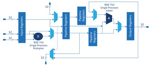
Recently, however, arithmetic FPGA signal processing options have taken another step forward with the introduction of hardwired floating-point embedded hardware. For example, Arria® 10 FPGAs are the industry’s first FPGAs and SoCs that natively support a single-precision floating-point DSP block mode as well as standard- and high-precision fixed-point computations using dedicated hardened circuitry. The single-precision floating-point DSP block mode is IEEE 754 compliant and comprises an IEEE 754 single-precision floating-point adder and IEEE 754 single-precision floating-point multiplier as shown in Figure 1. 1

Figure 1: Altera Single-precision Floating-point Mode DSP Block
As FPGAs such as Altera Arria 10 and Stratix 10 inevitably become cheaper, the choice of floating-point hardware naturally will become more prevalent and Centar’s floating-point FFT array-based architecture is well suited to reducing LUT/register fabric usage. 2
Comparison of Floating Point Implementations
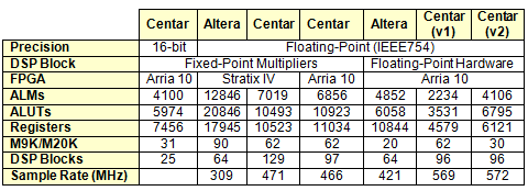
Here comparisons are shown in Table 1 for 1024-point, streaming FFT circuitry (normal order in/out) using two FPGA types and two levels of precision. The “Precision” category in Table 1 corresponds to either a fixed-point 16-bit input and output FFT circuit (first column) or circuits capable of achieving the high precision of the IEEE754 standard (other columns).
Without the embedded hardware support for floating-point arithmetic, the usual approach has been to simply increase fixed-point word lengths until the desired precision was reached 3. In this case fixed-point multipliers are used, as indicated in columns 2 through 4 of the “DSP Block” row. Two of the latter use Stratix IV EP4SE230F29C2 FPGAs (40nm technology). These circuits were compiled using Altera’s software tools (Quartus II v16.0) and the Altera design was based on IP Core v15. The Centar circuit in Column 4 is the same as that in Column 3, except that it was migrated to an Arria 10 FPGA. It was included to show the similarity in resource usage for Stratix IV and Arria 10 FPGAs. In this case different PLLs and fixed-point multiplier IP were used. Also, Arria 10 M20K memories were substituted for the Stratix IV M9K memories.
Finally, the last 3 columns correspond to FFT circuitry that uses the floating-point hardware in the Arria 10 DSP blocks. The circuits were compiled using Altera’s software tools (Quartus II v16.1) using an Arria10 10AS066H1F34E1SG FPGA (20nm technology) device and FFT IP v16.1. To illustrate the flexibility possible in choosing resources, two versions of the Centar circuit are shown: “v1” uses M20K memories for the internal FFT engine working memory and “v2” uses MLABs for this.
The TimeQuest static timing analyzer was used in all cases to determine maximum clock frequencies (Fmax) at 1.1V and 85C (worst case settings). The same Quartus settings were used for both the Centar and Altera designs. The Stratix IV FPGA adaptive logic module (ALM) is the basic logic cell unit (two 4-input adaptive LUTs, two registers plus other logic). In the Arria FPGA an ALM is two 4-input adaptive LUTs, four registers plus other logic.
For the Arria 10 FPGAs, the goal of the design approach was to minimize the usage of FPGA LUT/register fabric, since, as noted earlier, FPGAs are available in a variety of versions containing substantial numbers of embedded elements such as memory and arithmetic.

Table 1. Comparisons of resource usage and speed of different FPGAs and fixed/floating-point DSP block usage
Several important comparisons can be drawn from the numbers in Table 1:
- Use of the embedded DSP block floating-point hardware drastically reduces the need for LUTs, registers, and memory. For example, the Centar design (v1) compared to the Altera Stratix IV fixed-point multiplier implementation uses x5.9 fewer LUTs, x3.9 fewer registers, x5.8 fewer ALMs, and 30% fewer M20Ks.
- When comparing Centar’s (v1) Arria 10 design using the DSP floating-point hardware, the Altera equivalent uses x2.2 more ALMs, x1.7 more ALUTs, and x2.4 more registers. Centar “v2” trades off embedded memory (M20Ks) for LUTs, but still uses 15% fewer ALMs.
- Even a 16-bit, fixed-point FFT (Column 1) requires 69% and 63% more LUTs and registers compared to Centar’s (v1) circuit in the same FPGA technology, just to show there’s little rational for not using the floating-point hardware.
- For the same Arria 10 FPGAs, Centar circuits provide about 35% higher throughputs. This is due to the locality of interconnects associated with the nearest neighbor array structure and to a different algorithm for computing the DFT2
Centar FFT Architecture
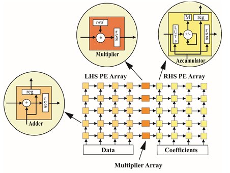
The key to reducing the LUT/register fabric usage when designing FFTs for Altera 10 FPGAs is to move as much of the processing into the embedded DSP blocks as possible. These DSP blocks provide several basic floating-point primitives: multiplication, accumulation and addition. Centar’s architecture focuses on doing exactly this in that it consists of an array of processing elements (PEs), each of which performs one of these simple primitive operations as shown in Fig. 1. Here the PEs on the LHS perform floating-point addition, the multiplier array PEs perform floating-point multiplication, and the RHS PEs perform floating-point accumulation with sums passed to memory “M” in Fig. 2.
Most of the registers used in the array structure support the fast systolic passing of coefficients and intermediate data between PEs, but about 17% are used to register inputs of the floating-point multipliers and might in the future be absorbed into the DSP block.
About 25% of the 2234 ALMs in Table 1 provide control needed to do many transform sizes. This number can be significantly reduced for single transform sizes.

Fig. 2. FFT architecture consisting of left hand side (LHS) 4x4 PE array, multiplier 4x1 PE array, and right-hand side (RHS) 4x4 array.
Conclusion
As FPGA models and technology continue to evolve, floating-point hardware in the DSP blocks will gradually replace traditional fixed-point FFT implementations, with substantial savings of design time and FPGA LUT/register fabric.
For real-time signal processing Centar’s FFT architecture is best suited to reducing LUT/register usage because the entire FFT engine can be reduced to the simple DSP floating-point primitives of multiplication, addition, and accumulation.
Since higher clock rates translate directly to higher throughput, Centar’s programmable, systolic, array-based architecture is inherently faster because connections are local and PEs are simple, Throughputs can be increased with larger arrays.
1 Hardened Floating-Point Processing in Arria 10 FPGAs and SoCs, https://www.altera.com/products/fpga/features/dsp/arria10-dsp-block.html
2 “High-Throughput Programmable Systolic Array FFT Architecture and FPGA Implementations”, http://centar.net/information_links/Nash_ICNC_2014.pdf
3 https://www.design-reuse.com/articles/37994/floating-point-fft-with-minimal-hardware.html
Related Semiconductor IP
Related White Papers
- How to build ultra-fast floating-point FFTs in FPGAs
- Floating-point emulation: faster than hardware?
- Floating-point FFT with Minimal Hardware
- FPGAs: Embedded Apps : Designing an FPGA-based network communications device
Latest White Papers
- Ramping Up Open-Source RISC-V Cores: Assessing the Energy Efficiency of Superscalar, Out-of-Order Execution
- Transition Fixes in 3nm Multi-Voltage SoC Design
- CXL Topology-Aware and Expander-Driven Prefetching: Unlocking SSD Performance
- Breaking the Memory Bandwidth Boundary. GDDR7 IP Design Challenges & Solutions
- Automating NoC Design to Tackle Rising SoC Complexity