Design of an image-processing device for cost-sensitive, high-volume applications using a novel dynamically reconfigurable technology
By Colin Dente & Dyson Wilkes, Akya Limited
Abstract
Many devices could benefit from programmability, but high-volume, cost-sensitive applications often force device manufacturers to use hard-wired RTL design techniques for reasons of end device cost. This results in the need for multiple silicon implementations to support different device variants, and means that device manufacturers are slow to respond to changing market requirements owing to the time taken to redesign, verify, manufacture and test a new device variant. Though programmability is highly desirable, the complete flexibility of function provided by a CPU or DSP-based solution is rarely necessary. This paper illustrates a design approach that uses a novel dynamically reconfigurable logic (DRL) technology to produce a device that is just reconfigurable enough to meet the flexibility requirements of the manufacturer whilst not imposing a significant size or power overhead compared to traditional RTL-based design techniques. Though illustrated using an image processing application, the techniques described are applicable to the majority of digital signal processing applications.
Structure of the paper
Section I – Motivation. Describes the design problem and Akya's “ART” dynamically reconfigurable logic technology.
Section II – Design. Describes the implementation of the design in two versions of ART, demonstrating the evolution of the technology and how DRL techniques simplify the design process.
Section III – Results. Provides details of the results of implementing the design in ART and a comparison to an implementation done in RTL.
Section IV – Conclusions.
Section V – References.
I. Motivation
I.1 Design problem
Akya Limited was approached by a manufacturer of image signal processing chips for mobile phone cameras to design a JPEG encoder that would be flexible enough to allow them to meet the constantly-changing requirements of their customers.
The design needed to be capable of encoding a large range of image sizes up to a maximum of 5M pixels at a rate of 15 frames per second. In addition to a large range of input image sizes and frame rates, a wide variety of output formats needed to be supported, including future formats which were unknown at the time of the design of the device.
I.2 ART DRL technology
Many previous (and current) attempts to produce a dynamically reconfigurable logic technology have sought to produce completely general-purpose fabrics consisting of regular arrays of relatively primitive processing elements (see [Master 04], [Duller 03] for examples). Whilst very good at providing significant general-purpose processing power, such approaches tend to lead to inefficiencies in terms of power and silicon area compared to customised hardware for any specific task as, inevitably, some portions of each general-purpose processing element will be unused for a particular application.
Akya's dynamically reconfigurable technology called “ART” was designed from the outset to target low-power, low-cost applications. Central to the design of ART was the desire to avoid, as far as possible, the overhead of redundant capability found in general-purpose architectures. For this reason, an ART-based design is tailored to a specific application area, resulting in a selection of processing resources which closely match the requirements of the algorithm or algorithms to be implemented, with very little overhead compared to a hard-wired RTL implementation of the same algorithm.
ART allows the designer to separate the design problem into two parts – the dataflow design and the control design. This simplifies the design process and allows shorter design times, and results in fewer errors in the design. ART works by allowing the designer to specify a highly reconfigurable datapath built from a library of standard signal processing functions (e.g. adders, multipliers, logic functions, registers, etc.). This datapath is then controlled and configured on a clock cycle-by-clock cycle basis by firmware which implements the control flow for the device.
ART devices are based around Reconfigurable Processing Matrices (RPMs) which consist of a reconfigurable datapath constructed from Processing Elements (PEs) selected from the ART PE library and a Reconfigurable Interconnect (RI) between the PEs, along with the control processing elements which control the operation of the PEs and the RI. The general structure of a typical ART RPM is shown in Figure 1.
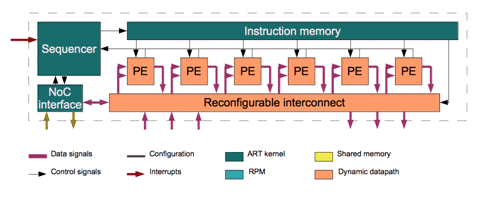
Figure 1 Structure of ART RPM
An ART-based device consists of one or more RPMs, along with shared memories (used for inter-RPM communication) and a network-on-chip (for inter-RPM communications and device configuration) connected together to form an ART Core. An example of an ART Core is shown in Figure 2.
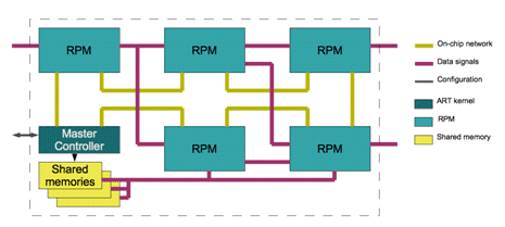
Figure 2 ART Core
Note that RPMs in an ART Core can communicate by any of three methods: Direct Interconnect, which provides any number of arbitrary-width signals between RPMs; the ART Token Ring Network-on-Chip, which is used to configure the device at power-on and to reconfigure the device whilst operating, and is available for communication between RPMs; and shared memories which allow RPMs to access a shared pool of memories which can be used to pass data between RPMs.
I.3 Advantages of DRL
The design requirements provided by the customer called for the ability to support a large range of image sizes, from quarter-VGA up to 5Mpixel, with a variety of different output formats – supporting different output data rates, strobe timings, padding, insertion of end-customer dependent meta-data, etc.
In addition, the device was required to use a single memory buffer for the eight-line image buffer (rather than using a conventional “ping-pong” double buffer). Implementation of such a single-buffer scheme requires fairly complex addressing for the memory, and support for multiple different input image sizes in such a scheme calls for significant flexibility in the address generation scheme. The software nature of ART's control firmware makes such a flexible implementation of a complex algorithm very easy compared to a fixed-function RTL implementation. In particular, the powerful looping and branching instructions available in the ART Interconnect Sequencer allowed for a highly efficient implementation of the address calculation.
In contrast to the difficultly of the eight-line buffer addressing, some other parts of the JPEG encoding algorithm were very simple in terms of control, though extremely computationally intensive. An example of this is the Discrete Cosine Transformation (DCT). To process a 5Mpixel image at 15 frames per second, a peak processing rate of around 1GOPS is required , but the processing is a simple repetitive loop which is performed on all the pixels in the image, requiring no control processing other than “start” and “stop”.
The device was also required to support dynamic modification of the quantisation tables used as part of the JPEG algorithm by the host CPU.
The quantisation step in the JPEG algorithm involves the division of each coefficient in an 8x8 block by a certain value. To avoid the need for a division operation, the quantisation values were converted to reciprocals so that a multiplication could be used instead. In addition, certain scale factors required by the DCT algorithm chosen (see Section II.4) were combined with the reciprocal quantisation constants in order to reduce the number of arithmetic operations to be performed.
Because the specification called for the ability to modify the quantisation tables “on-the-fly”, these values could not be pre-computed, so it was necessary to have computing resources available in the design to perform this function. Rather than having a dedicated multiplier available for this function, a multiplier that was otherwise used for the calculation of products required as part of the DCT algorithm was shared. Because the ART DRL approach explicitly separates the datapath and control design phases it is trivial to perform such resource sharing. This could be done in an RTL design, but the coding tricks required to convince a standard RTL synthesis tool that such a resource could be shared would be far from trivial.
II. Design
II.1 Initial prototype
The first JPEG decoder design we undertook, dubbed the “Akya Experimental JPEG Encoder”, or “AEJE” was developed at the same time as we developed the initial implementation of ART (ART1). The design was divided into four RPMs (see Figure 3).
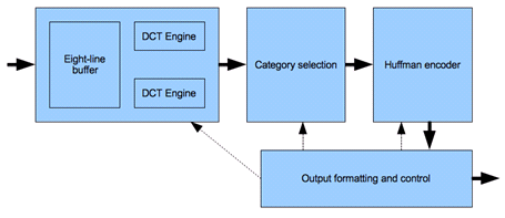
Figure 3 AEJE configuration
The first RPM was responsible for the eight-line buffer, DCT and quantisation, the second for category selection, the third for Huffman encoding, and the fourth for output formatting, CPU interface and overall control.
II.2 ART1 design issues
A feature of ART1 that was used extensively in the design of AEJE was the support for “Custom PEs” - i.e. PEs that just encapsulated user-written Verilog code. Whilst seemingly making it much quicker to implement complex functions, these Custom PEs caused significant issues in test, debug and code maintainability, and were a major source of delay during the project. As a result of this, the second generation of ART (ART2) has been designed to make the need for Custom PEs extremely rare, and a much more rigorous development and testing process is required before a Custom PE can be used in an ART2-based design.
Another feature of ART1 concerned the placing of registers. All “arithmetic” PEs such as adder/subtractors, Boolean functions and multipliers had sets of registers on their inputs that were used to provide operands for each arithmetic operation. This led to issues with access to operands required for multiple operations and with the correct sizing of the register files within the PEs – leading to a conflict between the desire for a minimal register file size and the desire to minimise the number of PE variants. This issue was solved in ART2 by moving all registers into separate register (or register file) PEs – making all arithmetic PEs purely combinatorial – thus greatly simplifying the issues of operand access, register file sizing and PE library complexity.
II.3 Second design - ART2
Following the successful completion of the AEJE design, Akya developed a second generation of ART (“ART2”) using the lessons learned in the development of ART1 and AEJE. The set of PEs developed for ART1 was examined and refined in order to create a clean, orthogonal set of PEs that would allow the efficient creation of designs. In order to handle cases where specialised functions were required, which would cause an unnecessary overhead of control inputs to PEs if constructed from the PE library and RI in the normal fashion, the concept of “Composite PEs” (CPEs) was introduced. These allow standard PEs to be connected together in a more-or-less fixed fashion, with the resultant composite structure appearing as a conventional PE to the rest of the ART device. This allows complex functions to be built with much lower verification requirements as they are constructed from pre-verified ART2 PEs. In addition, the ART “core” components such as the Interconnect Sequencer and network-on-chip were redesigned from scratch to give a cleaner, smaller and more modular implementation.
Once the design and implementation of ART2 was complete, we revisited the JPEG encoder design and implemented the Akya JPEG Core (“AJC”) using ART2.
As can be seen from Figure 4, the design was simplified, with the category selection and Huffman encode RPMs of AEJE combined into a single RPM. Experience gained from the experimental design led to an improved partitioning as show in figure 4. Akya engineers also optimised the mapping of the application onto cycle-by-cycle control of the Interconnect Sequencer. In addition, the output formatting and control RPM was extensively redesigned to improve flexibility and allow it to operate without the need for a host CPU (in fact, it is capable of performing the system control functions for the rest of the image signal processor which were formerly performed by the separate host CPU).
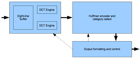
Figure 4 AJC configuration
II.4 DCT implementation
The algorithm used to implement the DCT was that of Arai, Agui and Nakajima [Arai 88]. This algorithm is described in Figure 5.
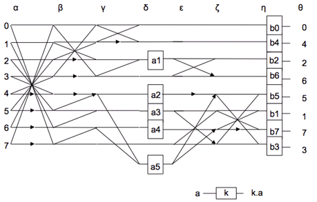
Figure 5 AAN DCT algorithm
The application of this 1D DCT algorithm to a 2D DCT is well known . We will consider a simplified case of implementing just a 1D DCT of 8 coefficients using this algorithm in order to illustrate the process of design and the advantages of the separation of data and control flow inherent in ART.
Inspection of Figure 5 shows that the algorithm requires 29 additions or subtractions and 5 multiplications (ignoring the “b” multiplications which are absorbed into the quantisation process in the 2D implementation).
Design constraints meant that one coefficient needed to be processed every clock cycle, thus, assuming that the basic hardware would be duplicated (for the horizontal and vertical components of the 2D DCT), a total of 8 clock cycles were available to perform a 1D DCT on 8 coefficients. Performing 29 additions or subtractions and 5 multiplications in 8 clock cycles requires a minimum of 4 adder/subtractors and 1 multiplier.
Adding a register file to hold intermediate values and a memory to hold processed results leads to the simplistic hardware requirements shown in Figure 6.
Note that in this diagram the small circles represent possible connectivity - so, for example, the inputs of the first adder/subtractor may connect to the outputs of any PE except itself.
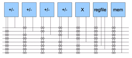
Figure 6 DCT RPM structure (simplified)
This hardware is encoded using ART Architecture Description language (AAD) as shown in the code fragment in Table 1.
Note that only two adder/subtractors and the multiplier are shown for the sake of brevity. The ellipses (...) indicate omitted code. The “y” input of the multiplier connects only to a register file that holds the “a” constants from the AAN algorithm – this is not shown in Figure 6.
It is important to note that the above description deals only with the hardware resources and the possible connections between them. No consideration needs to be given to the actual connections between PEs or the control signals to the PEs which will be used at a given instant (the control statements such as “op = add” and “signed_x = no” merely specify default values for these controls), as this is defined later by the ART firmware.
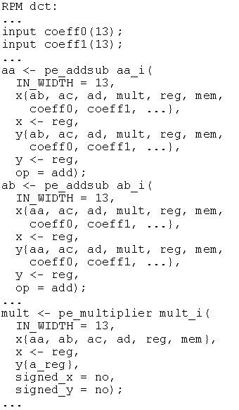
Table 1: Code fragment for DCT RPM
The AAD description of the hardware is processed by the ART design tools to produce a fully-synthesisable Verilog description targeted at either standard cell libraries or supported FPGAs as well as a SystemC simulation model.
Once the hardware description of the datapath is complete, the control portion of the design, implemented in ART firmware, can be written. In this description we will use ART Assembly Language (AAL) for the control description .
ART firmware is written by describing, for each clock cycle, the connectivity of the RI and the control values for the PEs. A fragment of AAL code for the implementation of the AAN algorithm on the hardware described in Table 1 is shown in Table 2.
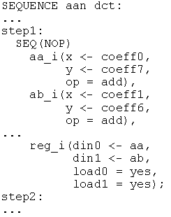
Table 2: AAL code for AAN algorithm
It can be seen that, for each PE, the connections to be made to each of its inputs are specified, along with the values of its control inputs. The “SEQ()” instruction specifies the opcode to be executed by the Interconnect Sequencer (ISEQ) during this clock cycle – in this case “NOP” – which simply advances execution to the next instruction on the next clock cycle .
When the firmware was written, it was found that it was impossible to schedule the required operations within the 8-clock cycle limit using only 4 adder/subtractors. For this reason, it was necessary to add a fifth adder/subtractor. In an RTL design, this would have resulted in a significant amount of coding to add the required resource and connect it up to the other resources in the design; however, using AAD the change was trivial – as shown in bold type in Table 3.
Following completion of the firmware, it became obvious that much of the possible connectivity described in the hardware was never used, as all operations were register – arithmetic – register or input – arithmetic – register. In addition, the arithmetic PEs only ever write to the memory, and do not need to be able to read from it.
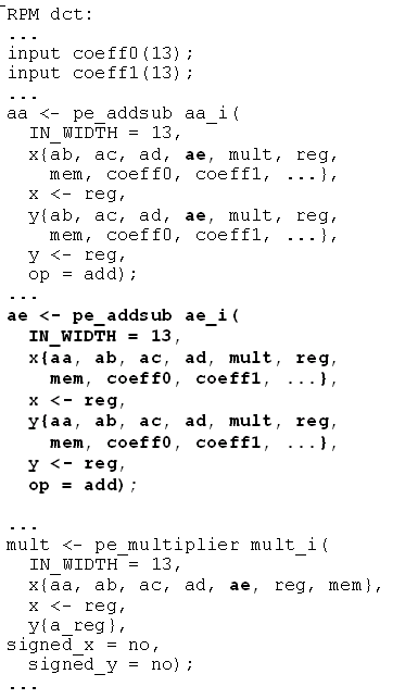
Table 3: Modification of DCT RPM to add fifth adder/subtractor
These redundant connections increase the size of the device in two ways: firstly, by increasing the complexity of the RI; and secondly, by increasing the number of bits in the instruction word required to control the RI. For this reason, the decision was taken to remove this redundancy.
As for the case of the addition of the fifth adder/subtractor, making such changes in RTL would be a lengthy and error-prone process, but it is trivial using AAD. The modified AAD is shown in Table 4.
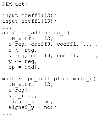
Table 4: DCT RPM with redundant connectivity removed
It should be noted that there is always a trade-off when removing redundant connectivity between reduction in the size of the resultant device and retention of reconfigurability. In the case of the DCT, where no changes to its function were considered likely, the minimisation of size was considered most important.
III. Results
The development of AEJE using ART1, though ultimately successful, took far longer than predicted, mainly due to the inclusion of custom Verilog code in “Custom PEs”. The resulting implementation (excluding the eight-line buffer memory) was approximately twice the size of a hand-coded Verilog implementation of the same function developed by our customer. It should be noted, however, that when the eight-line buffer memory was included in the size calculation, the ART1 implementation only increased the overall chip size by approximately 10%.
The ART2-based implementation of AJC took a total of 4 engineer-months from agreement of specification to signoff of the generated Verilog RTL for synthesis and layout.
AJC used approximately 63% of the logic and 67% of the memory required for AEJE (excluding the eight-line buffer) – giving an approximate overhead compared to a Verilog implementation of 20-30%.
A summary of the sizes of the three implementations of the function is given below. Note that these figures are approximate, and have been adjusted to account for changes in function between the versions of the design.
| Technology | Gates | Memory | Size | Overhead |
| ART1 | 2M | 170K | 5.0 | 100% |
| ART2 | 1.2M | 200K | 3.3 | 30% |
| Verilog | 1M | 80K | 2.5 | 0% |
Gates figure is in NAND2 equivalents. Memory is in bits and excludes the eight-line buffer. Size is in mm2 in 0.18µm silicon. Overhead is compared to Verilog implementation.
IV. Summary and conclusions
By restricting the reconfigurability of a solution to just reconfigurable enough (i.e. only enough reconfigurability to enable the possible function changes which will be needed) the use of dynamically-reconfigurable logic technologies can allow the creation of flexible, efficient devices which combine the programmability of a processor-based solution with the low power and low area cost of a hard-wired solution, allowing manufacturers to create devices able to respond quickly to changing market requirements and to combine multiple product variants into a single silicon implementation, thereby saving considerable development, testing and inventory costs. Additionally, a design process that allows the designer to separate the tasks of datapath design and control implementation leads to significantly reduced design time and fewer design errors. Akya's “ART” dynamically reconfigurable logic technology is an example of such a technology. These design techniques are applicable to a wide range of digital signal processing applications.
V. References
[Arai 88] Y. Arai, T. Agui, M. Nakajima, A Fast DCT-SQ Scheme for Images, Trans. of the IEICE. E 71(11): 1095 (Nov. 1988).
[Pennebaker 92] W. B. Pennebaker, J. L. Mitchell: JPEG Still Image Compression Standard, Springer, 1992.
[Master 04] P. L. Master, E. Hogenauer, W. J. Scheuermann: US Patent 6836839 - Adaptive integrated circuitry with heterogeneous and reconfigurable matrices of diverse and adaptive computational units having fixed, application specific computational elements, Published 2004.
[Duller 04] A. Duller, G. Panesar, D. Towner: Parallel Processing – the picoChip Way!, Communicating Process Architectures – 2003 Jan F. Broenink and Gerald H. Hilderink (Eds.), IOS Press, 2003.
Related Semiconductor IP
- NPU IP Core for Mobile
- NPU IP Core for Edge
- Specialized Video Processing NPU IP
- HYPERBUS™ Memory Controller
- AV1 Video Encoder IP
Related White Papers
- A Reconfigurable System featuring Dynamically Extensible Embedded Microprocessor, FPGA and Customisable I/O
- High Speed Connected Component Labeling as a Killer Application for Image Recognition Systems by Dynamically Reconfigurable Processor
- Proposal of a Dynamically Reconfigurable Processor Architecture with Multi-Accelerator
- Reconfiguring Design -> Reconfigurable computing aims at signal processing
Latest White Papers
- Ramping Up Open-Source RISC-V Cores: Assessing the Energy Efficiency of Superscalar, Out-of-Order Execution
- Transition Fixes in 3nm Multi-Voltage SoC Design
- CXL Topology-Aware and Expander-Driven Prefetching: Unlocking SSD Performance
- Breaking the Memory Bandwidth Boundary. GDDR7 IP Design Challenges & Solutions
- Automating NoC Design to Tackle Rising SoC Complexity