A Reconfigurable System featuring Dynamically Extensible Embedded Microprocessor, FPGA and Customisable I/O
by Michele Borgatti, Francesco Lertora, Benoit For& and Lorenzo Cali
STMicroelectronics
Innovative Systems Design, NVM-DP, Central R&D
Agrate Brianza (MI), ITALY
Abstract
A system-chip targeting image and voice processing and recognition application domains is implemented as a representative of the potential of using programmable logic in system design. It features an embedded reconflgurable processor built by joining a configurable and extensible processor core and a SRAM-based embedded FPGA. Application-specific bus-mapped coprocessors and flexible I/0 peripherals and interfaces can also be added and dynamically modified by reconflguring the embedded FPGA. The architecture of the system is discussed as well as the design flows for pre- and post-sil&on design and customisation. The silicon area required by the system is 20mm2 in a 0.18urn CMOS technology. The embedded FPGA accounts for about 40% of the system area.
Introduction
These days we are witnessing two conflicting trends in the electronic industry. At one side the economics of system integration pushes logic suppliers towards ever more complex system-chip devices. On the other side, increasing complexity of design and associated risks, increase of non-recurrent engineering expenses and shorter time-to-marked and product life are causing OEMs to look for faster turnaround and lower risk design solutions and technology.
The recent introduction of embedded programmable logic allows ASIC and ASSP vendors to broaden the appeal of their products. Also, hardware programmability can be exploited by system integrators for product customisation.
In this paper we present a pragmatic approach to introduce flexibility in system-chip design and exploit embedded programmable silicon fabrics to enhance system performances. In particular, enabling application-specific configurations to adapt the underlying hardware architecture to time-varying application demands can improve execution speed and reduce power consumption compared to a general-purpose programmable solution. In the proposed system the embedded programmable logic allows static or dynamic configuration of the instruction set of an embedded microprocessor, the creation of busmapped application-specific hardware coprocessors and accelerators, and the customisation of the system I/O. The latter feature allows the device to potentially connect to any extemal unit/sensor given that its communication protocol can be mapped to the on-chip programmable logic. Also, some computations can be performed on-the-fly when data is captured.
The proposed system has been built using a set of state-of-theart IP cores and system design methodology. In particular, a configurable and extensible processor (1) with associated tools, and an embedded FPGA (2) were used. The resulting system has been developed to target image and voice processing and recognition application domains. Design flows for system exploration and implementation are also introduced.
System Architecture
One of the main goals of this work was to build a flexible architecture, working at a reasonable high clock frequency, built around an embedded FPGA and an extensible 32-bit microprocessor.
The base processor is a specific customisation of that described in (1). It comes with a complete set of tools for configuration and performance analysis. Main features of the processor core used in our system are: 5-stage pipeline, 8+8kB direct-mapped data/instruction caches, a 24 or 16 bit instruction format for improved code density, a 64 bit processor interface (PIF) with burst transfers for cache-page refill, 13 interrupt lines organized in 4 priority interrupt levels.
The system architecture is illustrated in Fig.1. The PIF/AHB Bridge translates processor cycles to the AMBA AHB bus (3) with support for fast burst and locked transfers. An external memory interface (EMI) exploits the available peak throughput of fastest commercial external non-volatile flash memories. It allows a wide range of burst mode and page mode configurations under software control and supports low-voltage, low-swing operations. If required, an external RAM port allows the extension of the on-chip 48kB SRAM. The heart of the system is an embedded FPGA and its multiple interfaces to main system units, in particular the functional purposes of the e-FPGA programmable logic are:
- extension of the processor datapath supporting a set of additional special-purpose instructions (TIE). This is done by connecting the processor datapath through a wide bus and a specific interface (TIE bus/interface in Fig. 1);
- bus-mapped coprocessor. Hardware units mapped into the e-FPGA can be interfaced to the system bus through an AHB bus master/slave;
- flexible I/O. The programmable general-purpose I/O pads interface is used to connect external units or sensors with their application-specific communication protocol.
All these possibilities may be mixed in a singular configuration for the FPGA and this results in a highly configurable device. To accelerate communications between the configurable hardware and software tasks running on the processor, 4 interrupt channels can be driven by logic mapped into the e-FPGA. A two-way HW/SW communication can be implemented by the joint usage of these interrupt channels and dedicated AMBA APB registers.
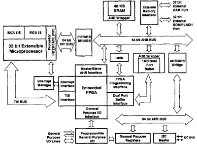
Fig. 1: System Architecture Block diagram
Download of the FPGA bitstream is performed by a flexible programming interface. To allow validation of the FPGA configuration, the bitstream may be read-back by hardware support.
Most audio or video applications require storage buffers to interface fast decoding hardware and slower software running on-the processor. With this concept in mind, a lkByte dual port buffer has been added and organised as 4x256 bytes rows. One port of this buffer is connected to the AHB bus while the second port is directly accessed by the FPGA dual port buffer interface.
The AMBA APB Bus connects all the configuration/general purpose registers to the system. On the same bus, an I2C master interface has been added to connect external devices or sensors like LCD display, CMOS camera, etc...
A programmable general-purpose I/O module features mono input/output and bi-directional pads under the control of both the e-FPGA and the microprocessor.
A. The Microprocessor-FPGA interface
The configurable processor allows adding user-defined instructions. In the proposed architecture, this capability was mapped exclusively into the e-FPGA, allowing runtime re-configuration of the instruction set. This implies that the number of user-defined instructions available at a given time is limited by the e-FPGA logic capacity and instruction logic complexity. However, a set of additional instructions can be defined to target specific application needs. If the logic size of the set of additional instructions exceeds the logic capacity of the e-FPGA, it might be split into a number of contexts fitting the size constraints of the e- FPGA. These contexts might be used to dynamically reprogram the FPGA to support application needs.
The flexibility advantage of this architecture implies a speed penalty for the part of logic mapped inside the e-FPGA. In particular, specific processor instructions mapped in the reconfigurable fabric may be lx to 10x slower than their equivalent implementation in standard cells.
Fig.2 details the processor-FPGA interface: a focus is given on how Instruction Extensions are mapped inside the FPGA and how synchronisation between the microprocessor and the e-FPGA is guaranteed.
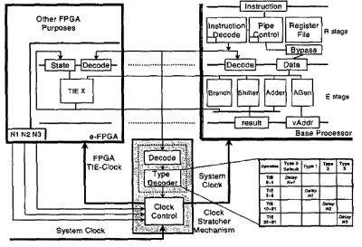
Fig. 2: Embedded FPGA - Microprocessor Interface
As the additional instruction set is part of the processor pipeline (1), slowing down this logic results in a drastic reduction of processor maximum speed hence affecting processor performance when using the baseline generalpurpose instruction set.
A mechanism is introduced to allow the processor to be clocked at its maximum speed while executing standard instructions, whereas it is slowed down by a programmable, instruction-dependent number of cycles (1-16) when executing processor instructions mapped into the FPGA.
A clock control system allows the processor to be synchronised with the e-FPGA for the number of cycles the instruction is executed. A dedicated module is able to identify instructions whose performance is not aligned with the processor. As each of these instructions needs to be associated to its execution time, the set was partitioned. A pre-defined map-table divides in 4 the whole set of opcodes reserved for user-defined instructions.
For each set that belongs to a configuration, a number, mapped as a constant output of the FPGA, defines the number of times the clock needs to be stretched to synchronise properly the execution of the pipeline between the FPGA and the base processor. Thus, the system allows executing a set of TIEs among a panel of 4 user-defined speed penalties for any FPGA configuration. In this way, the processor CPU is tied to the FPGA speed for the strictly required number of cycles. The set of user-instructions can be defined after tape out thanks to the FPGA. More, the system allows to parametrise its execution time, to exploit the performances of both hard-wired and programmable logic.
B. Block Description of the e-FPGA
The architecture of the e-FPGA (2) is organised as a hierarchical multi-level interconnect network (see Fig.3)
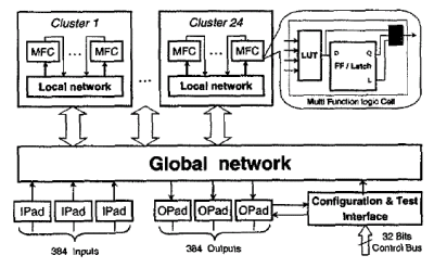
Fig. 3: Block diagram of the e-FPGA
An array of logic elements called Multi Function logic Cell (MFC) allows implementation of digital logic. The MFC is a 4 input / 1 output programmable structure associating a 4 input Look-Up Table and a storage element (dff, latch). There are 3k MFC shared among 24 clusters. The Global Interconnect Network links the clusters together and to IPads & OPads peripherals cells. At a lower level, a Local Interconnect Network links MFC together and to the global network. The architecture allows defining up to 1 clock signal per cluster. The MFC clock is one of 3 global signals defined to be connected to any input of the cluster. This insures a low skew between cluster clocks and a full IO assignment flexibility. The input (respectively output) pin set counts 384 independent and fully equivalent inputs (respectively outputs).
Design Flow and System Integration
A. The System-to-RTL design flow
In Fig.4 the design flow used for system architecture exploration and integration is described. The starting point is an untimed model of the system written in C/C++ code describing the desired functionality; at this stage the verification is done with simulations in CoWare N2C environment (4). This methodology allows designers to validate the system specifications and consequently, with a progressive refinement of the functional blocks into hardware and software (partitioning process) and the generation of the HW/SW interface (interface synthesis), the verification of the system at a cycle accurate abstraction level. The microprocessor core is abstracted in the coverification with its Instruction Set Simulator integrated into the simulation engine. Extensive simulations of the system with the usage of the profiler (memory accesses, cpu load, exceptions) help in finding the computational kernels of the software running on the core (performance analysis).
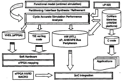
Fig. 4: System to RTL
At this point it is possible to group segments of codes that result timing consuming as new instructions of the extensible processor.
Those extensions of the Instruction Set can be easily mapped on the e-FPGA as well as the VHDL code that results from the refinement process done during partitioning phase. The system integration flow ends producing:
- Soft Hardware to be mapped on the eFPGA: HDL RTL code of instruction extensions, bus-mapped coprocessors and special purpose I/O peripherals.
- Conventional fixed hardware: Microprocessor RTL code, AHB/APB bus and Peripherals.
- Embedded Software (C code): Application software and low-level drivers for the hardware platform.
The C code generated by the flow described above became the final application while the RTL of the system with the e- FPGA hard macro goes into the system integration flow.
B. The RTL-to-Layout design flow
In the Fig.5 both silicon implementation flow and e-FPGA configuration flows are shown. These flows are run at different times. Once silicon implementation flow has produced the routed database its possible to implement e- FPGA flow that can be repeated for each different function built as a soft macro.
The RTL code of the CPU core, IP blocks and Interface modules (system bus) is synthesized and integrated with RAM blocks and FPGA hard macro in the fioorplanning environment. To meet timing requirements at the boundary of the e-FPGA, a special care was taken during synthesis process for the logic cells that interfaces e-FPGA with the rest of the system. A particular set of constraints was specified to reach minimum delay of the hardwired logic. After the place and route stage, the final database is statically and dynamically verified against the RTL simulations in order to make verification at all levels of abstraction.
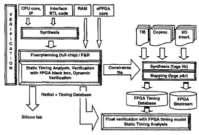
Fig. 5 RTL to Layout
The timed database used for the verification, built after a paracsitic extraction and a delay calculation process, allows knowing the effective delays at the boundary of the e-FPGA hard macro (all e-FPGA I/O pins are characterized with the static timing analyzer in the worst case condition). This information is exported in the e- FPGA flow as a constraint file and used during synthesis/mapping of the soft hardware by specific e- FPGA tools. This is done to correctly constrain the logic mapped on the e-FPGA with the real timing budget. Finally the generation of the bitstream and a timed view of the macro can be used for the final sign-off. Static timing analysis of the e-FPGA results in both a backannotated netlist and a timing view for full chip static timing analysis.
System Implementation and Test
The full-chip has been implemented in a standard CMOS 1.8V/3.3V, 0.18um technology featuring 6 metal layers. The layout of the system has been integrated using commercial place and route tools for digital ASIC. To avoid external multiple power supply, an internal DC (3V to 1.8V) voltage regulator has been integrated. The chip is being tested and is fully functional at the clock rate of 175MHz. The processor system is able to reconfigure the e-FPGA at full speed. Reconfiguration takes about 500us at a clock rate of 100MHz. During reconfiguration the average throughput sustained by external memories, EMI and programming interface is 50MB/sec. Device performances and power consumption are summarized in Table I. Technology and device characteristics are summarized in Table II and a chip micrograph is shown in Fig.6 with a floorplan view of system components. The system is being tested using both a face recognition application and a speech recognition application. During architecture development we reported speedups of 4x to 8x using instruction extensions to accelerate facerecognition computing kernels. Additional 1.5x to 2x performance improvements are reported on specific I/O intensive tasks to interface an external CMOS camera and doing some image processing computations on-the-fly using the e-FPGA.
Acknowledgements:
The authors thank Sara Bocchio, G. Repetto, C. Gazzina and L. Fumagalli for their valuable help and support. They also thank O. Lepape, J. Barbier and F. Reblewsky at M2000, J. Massingham and B. Campbell at Tensilica, and K. Ahluwalia, D. Tilley, M. Woodward and P. Bingham at CoWare. A special thank to Dr. A. Kramer for his support and encouragement.
TABLE I
DEVICE PERFORMANCES AND POWER CONSUMPTION
| Processor maximum speed | 125MHz (WCMIL) 175MHz (TYP) |
| Reconfiguration speed | ~500us @ 100MHz clock |
| Chip average power consumption | ~300mW @ 100MHz, 1.8V |
TABLE II
TECHNOLOGY AND DEVICE CHARACTERISTICS
| Technology | 0.18~xm CMOS 6-ML |
| SRAM Memory | Main: 48kB (64-bit wide) I$: 8kB (64-bit wide) D$: 8kB (64-bit wide) Buffers: 4x256B (8-bit wide) |
| Chip size | 5.5x5.5 ram2 (pad limited) |
| Core Size | 20 ram2 |
| e-FPGA size | 8.2 ram2 (15k useable equivalent ASIC gates) |
| Customisable I/O | 24 general-purpose inputs 24 general-purpose outputs (tristate) 8 general-purpose bidirs |
| Power Supply | 2.7-3.6V (external), 1.8V(core, internally generated / regulated) |
References
(1) R.E.Gonzalez., "Xtensa: A Configurable and Extensible Processor", IEEE Micro, March-April 2000, pp. 60-70.
(2) M2000, "Flexeos family technical manual", www.m2000.fr
(3) ARM Ltd., "AMBA TM Specification" Rev 2.0"
(4) I.Bolsens, H.De Man, B. Lin, C.Van Rompaey, S.Vercauteren and D.Verkest, "Hardware/Software Co-Design of Digital Telecommunication Systems", Proceedings of the IEEE, Vol. 85, No. 3, March 1997, pp 391- 418.
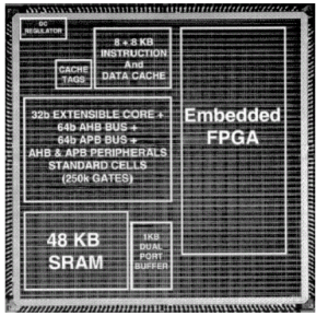
Fig.6 Chip Micrograph
Related Semiconductor IP
- NPU IP Core for Mobile
- NPU IP Core for Edge
- Specialized Video Processing NPU IP
- HYPERBUS™ Memory Controller
- AV1 Video Encoder IP
Related White Papers
- Emerging Trends and Challenges in Embedded System Design
- New Realities Demand a New Approach to System Verification and Validation
- Paving the way for the next generation of audio codec for True Wireless Stereo (TWS) applications - PART 5 : Cutting time to market in a safe and timely manner
- System on Modules (SOM) and its end-to-end verification using Test Automation framework
Latest White Papers
- Ramping Up Open-Source RISC-V Cores: Assessing the Energy Efficiency of Superscalar, Out-of-Order Execution
- Transition Fixes in 3nm Multi-Voltage SoC Design
- CXL Topology-Aware and Expander-Driven Prefetching: Unlocking SSD Performance
- Breaking the Memory Bandwidth Boundary. GDDR7 IP Design Challenges & Solutions
- Automating NoC Design to Tackle Rising SoC Complexity