Proposal of a Dynamically Reconfigurable Processor Architecture with Multi-Accelerator
Syuhei Igari, Junji Kitamichi, Yuichi Okuyama and Kenichi Kuroda, The University of Aizu
Aizuwakamatu JAPAN
Abstract:
The progress of LSI manufacturing technology has realized large-scale systems on a single chip, such as a System on a Chip (SoC) in recent years. In the field of embedded systems, the SoC has problems related to increasing in the scale of circuits and reducing the design costs, due to many types of application specific hardware modules. We expect that these problems can be overcome by reconfigurable devices such as Field Programmable Gate Arrays (FPGAs). Some of FPGAs can change circuit configuration dynamically while the system is running. In this paper, we propose a dynamically reconfigurable processor architecture with a multi-accelerator using Dynamic Partial Reconfiguration (DPR) technology by XILINX. The proposed architecture consists of a processor, some memories, some buses, controllers and some dynamically reconfigurable accelerators. We employ a multi-bus system and design the controllers for a dynamically reconfiguration. A JPEG encoder and decoder that are open-source IPs are used as target applications. The proposed architecture is implemented on a Virtex-6 FPGA and evaluated regarding the circuit size and reconfiguration time. The results showed that the partial reconfiguration time was small enough.
1. Introduction
The progress of LSI processing technologies has realized large-scale systems on a single chip, such as the System on a Chip (SoC). The SoC has some advantages such as the reduction of the number of LSIs and speed-up of communications by decreasing distance between circuits, and so on. In the field of embedded systems, the SoC needs to contain many types of application-specific modules to fulfill a wide variety of user-demanded functions. Thus, the SoC has problems related to the scale expansion of circuits and the increase of design cost.
It is anticipated that these problems can be overcome by exchanging a part of the SoC's functions using reconfigurable devices. The reconfigurable device has the function of reconfiguring hardware construction. Currently, many researchers are researching the devices such as STP Engine[1], MuCCRA[2], and so on. These are coarse-grained reconfigurable devices based on an ALU and have the advantage of quick reconfiguration by a multi-context system. On the other hand, Field Programmable Gate Arrays (FPGAs) are fine-grained reconfigurable devices based on a Look Up Table (LUT). The FPGAs are low-cost chip with large flexibility for design by HDL. However, the device has the disadvantage of requiring considerable time for reconfiguration.
Therefore, in this research, we propose a design method of a processor architecture to minimize the reconfiguration time using FPGA. The proposed architecture is designed using Dynamic Partial Reconfiguration (DPR)[3] technology provided by XILINX. The DPR is implemented in a family of FPGA provided by XILINX and can reconfigure a particular part without stopping the operations of other parts. A small-scale hardware is expected to have multiple functions by switching some modules in the same region and using different functions, which will partially reduce the reconfiguration time.
In this paper, we propose a dynamically reconfigurable processor architecture with a multi-accelerator. Using the proposed architecture, a multi-accelerator can be implemented on multiple regions according to the applications. The target application is a JPEG; an encoder and a decoder of open-source hardware are used. The proposed architecture is designed using an integrated development environment provided by XILINX and is implemented on a Virtex-6 FPGA. We design a controller with multiple ports corresponding to a multi-bus system. Streaming input and output data can be transferred without competition of bus access, and the data transfer delay of the system bus is minimized. The proposed architecture is evaluated regarding the circuit size and the reconfiguration time of each accelerator and the availability of the partial reconfiguration is validated by comparing the processing time. As a result, the partial reconfiguration time of JPEG encoder is sufficiently small, and the reconfiguration of the JPEG encoder is efficient.
2. Dynamic Partial Reconfiguration
Dynamic Partial Reconfiguration (DPR) technology provided by XILINX is described. Currently, DPR is used in many studies, such as cryptography processing[4], image processing, fault-tolerant systems and software radio. In a DPR system, hardware modules that are partially reconfigured are called Partially Reconfigurable Modules (PRMs), and the region where a PRM module is configured is called a Partial Reconfigurable Region (PRR). A bit stream file that contains the configuration data of PRM is called a Partial Bit Stream (PBM). The region that is not the PRR is called the Static Region, and the circuits which are configured in the Static Region, are not reconfigured while the system operates and continue the operation during any PRR reconfiguration. To reconfigure the PRMs, a primitive module called an Internal Configuration Access Port (ICAP) is used.
XILINX provides an integrated development environment ISE Design Suite in Figure 1.
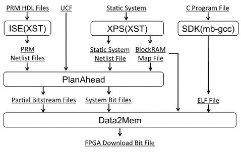
Figure 1. Design Flow using XILINX Development Environment
The ISE Project Navigator (ISE) manages design. PRMs are designed in Verilog HDL or VHDL and are synthesized to a netlist file using Xilinx Synthesis Technology (XST). The Xilinx Platform Studio (XPS) is a part of a function of the Embedded Development Kit (EDK). Using XPS, an embedded processor, such as MicroBlaze or PowerPC can be used.
The designed Static Module is synthesized by XST to a netlist file and a BlockRAM mapping file. In this process, the user IPs controlling the reconfiguration and operation of the PRM are designed. The user IPs contain the controller which manages the behavior and reconfiguration of the accelerator and the partially reconfigurable accelerator of PRM. Then, PRMs are defined as only an external interface and designed as black box modules without internal logic.
A Software Development Kit (SDK) is a part of a function of EDK. Using SDK, C program running on the embedded processor is implemented. The program is compiled by dedicated compilers to an Executable and Linkable Format (ELF) file. PlanAhead is a floor planner. First, the PR (Partial Reconfiguration) Project is made, and the netlist of the Static Module and an User Constraints File (UCF) for the target device are loaded. Then, the PRM netlist file is allocated to PRM designed as a black box in the Static Module, and PRR is laid out. The designed system is implemented after setting the BlockRAM mapping file, and the partial bit stream files of each PRM and the files of all system including PRM are generated. Using Data2MEM, various files generated by each tool are assembled into a bit stream file for initializing FPGA.
3. Proposed Dynamically Reconfigurable Processor Architecture with a Multi-Accelerator
We describe a dynamically reconfigurable processor architecture with a multi-accelerator, called a Partially Reconfigurable (PR) Multi-Accelerator. A multi-accelerator can be reconfigured and execute on multiple regions for accelerators depending to the applications. The proposed architecture consists of a processor, controllers and partially reconfigurable multiple regions for the multi-accelerator. Each accelerator is implemented on each region and can be reconfigured at independent times and be specialized for streaming processing. The proposed architecture has two features, a multi-bus system and PR Controllers. Using the multi-bus system, the ability of processing of an accelerator can be used at the maximum because streaming input and output data can be transferred without the competition of bus access and the transfer delay of a system bus is minimized. A dedicated controller for dynamic reconfiguration, which is called a PR Controller, manages the reconfiguration and the execution of an accelerator. Figure 2 shows the block diagram of the proposed architecture.
A PR Accelerator module has a PR Controller and a partially reconfigurable region. The multi-bus system has six buses: a bus connected to a processor and an instruction memory, a bus plb_bus connected to a MicroBlaze processor, data memory, and slave ports for each PR Accelerator, and four buses separately connected to four master ports of each PR Accelerator. Each bus is connected to multiple buses to avoid data-access conflict. The processor is connected to an instruction memory via the Local Memory Bus (LMB). Another bus is the Processor Local Bus (PLB). The processor writes control data to control registers via the slave port of the PR Controller or reads from control registers. If the reconfiguration and execution of an accelerator are finished, a PR Controller sends an interrupt signal. The processor detects the interrupt signal. The read master port of a PR Controller is connected to a bus with two memories for application data and partial reconfiguration data. The write master port of a PR Controller is connected to a bus with a memory for application data. In this way, the processing ability of an accelerator can be used at the maximum because streaming input and output data can be transferred without the competition of bus access and the transfer delay of a system bus is minimized. Each memory for application input and output data and partial reconfiguration data has a dual-port memory controller. A processor and a host PC can access these controllers by connection with mb_plb, which is connected to a processor.
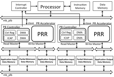
Figure 2. Block Diagram of the Proposed Dynamically Reconfigurable Processor Architecture with a Multi-Accelerator
3.1 PR Controller
A PR Controller is a controller which has multiple ports connected with a multi-bus system. Using a PR Controller, the reconfiguration and the execution of an accelerator are managed. A PR Controller contains a slave port, two master ports, control registers, two DMA units for read-only and write-only, three asynchronous FIFOs and an ICAP. Figure 3 shows the block diagram of the PR Controller.
DMA units are used for burst transfer via each master port. Using 32-bit width and 64 depth asynchronous FIFOs for these transfers, an accelerator, an ICAP, and a processor system can operate at different clock frequencies, and each part operates at each maximum operating frequency.
The states of PRM are referred as follows. To reconfigure a PRM, first, one of the control registers is set to transfer the burst read data to ICAP. The source address and the partial reconfiguration data size of memory in which the partial reconfiguration data is stored are written to one of control registers. Then, a burst read starts. The burst read data is transferred to ICAP via the FIFO for ICAP, and PRM is reconfigured. When the burst read is finished and the FIFO for ICAP is empty, the reconfiguration is finished, and an interrupt signal is activated. The processor receives the interrupt signal and invokes an interrupt handler programmed. To refer to the PRM status, the data of status register, which is one of the control registers, is read.
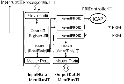
Figure 3. Block Diagram of PR Controller
To execute PRM, the source address of memory where the application input data is stored, the destination address of the memory where the application output data is stored, and the application input data size are written to the control registers. Then, a burst read starts. The burst read data is transferred to PRM via the FIFO for input PRM and processed sequentially. Output data from PRM, burst write data, is transferred via the output FIFO. If the PRM execution is finished, an interrupt signal is sent to the processor.
3.2 Partially Reconfigurable Modules
The Partially Reconfigurable Modules (PRMs) implement streaming processing, such as signal processing or image processing. Figure 4 shows the block diagram of PRM.
The PRM consists of an accelerator and a PRM Interface, which has a dedicated controller and memory for the input data stream.
We adopt JPEG (Joint Photographic Experts Group) encoding and decoding as the target application. The JPEG encoder and decoder are selected in OpenCores[5]. These modules can operate for the image format VGA(640x480). Huffman encoding and decoding are used as the entropy method, and the quantization table is 50\% image quality. We modify the interfaces of the encoder and decoder to be used as PRM.
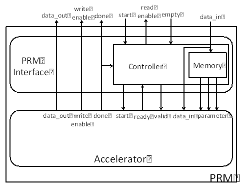
Figure 4. Block Diagram of PRM
4. Evaluation of Proposed Architecture
For the evaluation of the proposed architecture, the circuit sizes of PRRs and PRMs and the reconfiguration times are examined. The proposed architecture is designed using ISE Design Suite 12.3. The target device is a Virtex-6 (VC6VLX240T) mounted on an ML605 Evaluation Kit. Figure 5 shows the floor plan of the proposed architecture. In a target device, two ICAPs are allocated in the center. Each PR Controller is located at regions PRR-A and PRR-B, which are the JPEG encoder and decoder, respectively. Each PRR is located at the side of each PR Controller. A processor system operates at 125MHz, and ICAP and the JPEG encoder and decoder operate at 100MHz
Table 1 shows the PRR-A and PRR-B resources, each PRM resource, partial bit stream data size, and the reconfiguration time. The percentages of PRM in these tables show the percentages of PRR configuring the PRM. The reconfiguration time is measured from the time when the MicroBlaze sets a reconfiguration flag of a PR Controller to the time when the PR Controller sends an interrupt signal of reconfiguration completion.
The partial bit stream data sizes of the JPEG encoder and decoder are about 740Kbyte and 270Kbyte, and the reconfiguration times are 2.694ms and 0.986ms, respectively. The processing time of 1-frame JPEG encoding is 7.353ms. Then, the reconfiguration of the JPEG encoder is 0.37 times of 1-frame JPEG encoding. If multiple frames are processed using the same encoder, the overhead can be ignored. The reconfiguration time of the JPEG decCoder is 0.986ms and the time is shorter than that for the encoding.
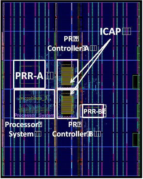
Figure 5. Floor Plan of Proposed Architecture
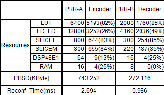
Table 1. PRR and PRM resources, partial bit stream data sizes and reconfiguration times
As a reference, the value of the reconfiguration time by XILINX is obtained from partial bit stream data size divided by the ICAP maximum throughput. In this experiment, the ICAP operates at 100MHz, and the ICAP data port is 32-bit data width. The maximum throughput is Bit Width * Frequency = 3,200 [Mbps]. The estimation values of reconfiguration times on PRR-A and PRR-B are 1.85[ms](= 743,252[Kbyte] / 3,200[Mbps]) and 0.68[ms](= 272,116[Kbyte] / 3,200[Mbps]), respectively. The rates between the reference values and the actual measured reconfiguration times are about 1.45. We believe the cause to be the delay of burst transfers of partial bit stream data through the asynchronous FIFO.
Table 2 shows the resources of a PR Controller. The resources of a PR Controller are smaller than those of other modules.
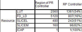
Table 2. Resource of a PR Controller
We have been implementing other PRMs which implement an H.264 encoder and decoder in OpenCores. An H.264 decoder cannot be implemented as a PRM because it has clock generation logic and Xilinx synthesis tools cannot synthesize such circuits. To implement the H.264 decoder, the architecture is significantly changed.
5. Conclusion
In this research, we proposed a processor architecture in which a multi-accelerator can be implemented on partially reconfigurable multiple regions depending on the applications. The proposed architecture was implemented on a Virtex-6 FPGA. We employed a multi-bus system available for streaming processing and designed controllers connected with multi-bus system. As accelerators, JPEG image processing is selected. As a result, the partial reconfiguration time of JPEG encoder is sufficiently small. The reconfiguration overhead can be ignored.
Our future studies include following. When partial bit stream data is stored in the external memory, the BlockRAM needs to be used as cache memory because the partial bit stream data size of about 740Kbyte is larger than the BlockRAM size. To use three PRRs or more, the architecture needs to be changed to control multiple PRRs using an ICAP only.
References
[1] Masato Motomura, "C-based Programmable-HW Core:STP Engine: Current Status and Future,'' in IEICE Technical Report, RECONF2008-48, 2008.(in Japanese)
[2] H. Amano, Y. Hasegawa, S. Tsutsumi, T. Nakamura, T. Nishimura, V. Tanbunheng, A. Parimala, T. Sano, and M. Kato, "MuCCRA chips: Configurable dynamically-reconfigurable processors,'' Asia and South Pacific Design Automation Conference (ASP-DAC) 2007., pp.384-387, 2007.
[3] Partial Reconfiguration User Guide, UG702(v12.3), XILINX, Inc., October 2010.
[4] Y. Hori, A. Satoh, H. Sakane, and K. Toda, "Bitstream encryption and authentication with AES-GCM in dynamically reconfigurable systems,'' International Conference on Field Programmable Logic and Applications (FPL'2008), pp.23-28, September 2008.
[5] "OpenCores,'' http://opencores.org/.
Related Semiconductor IP
- NPU IP Core for Mobile
- NPU IP Core for Edge
- Specialized Video Processing NPU IP
- HYPERBUS™ Memory Controller
- AV1 Video Encoder IP
Related White Papers
- High Speed Connected Component Labeling as a Killer Application for Image Recognition Systems by Dynamically Reconfigurable Processor
- High-Performance DSPs -> Processor boards: Architecture drives performance
- An Embedded Processor Architecture With Extensive Support For SoC Debug
- A Reconfigurable System featuring Dynamically Extensible Embedded Microprocessor, FPGA and Customisable I/O
Latest White Papers
- Ramping Up Open-Source RISC-V Cores: Assessing the Energy Efficiency of Superscalar, Out-of-Order Execution
- Transition Fixes in 3nm Multi-Voltage SoC Design
- CXL Topology-Aware and Expander-Driven Prefetching: Unlocking SSD Performance
- Breaking the Memory Bandwidth Boundary. GDDR7 IP Design Challenges & Solutions
- Automating NoC Design to Tackle Rising SoC Complexity