DDR2 Signal Integrity
Introduction
GDA System Engineering has been designing around complex memory subsystems for nearly ten years. As more and more devices are packed into a single board, it is becoming equally more desirable to eliminate the SODIMM connector and integrate memory devices. Designers today face the challenge of integrating DDR2 memory devices onto the same PCB while using the correct termination to ensure signal quality. This is applicable to any embedded platforms integrating high performance DDR2 memory subsystems.
At this point, DDR2 memories are available with clock speeds of 200MHz. (DDR2-400), 266MHz. (DDR2-533), and 333MHz. (DDR2-667). At such high speeds, one cannot take the risk of using a conventional design approach suitable for speeds of 133MHz. SDRAM and ignore the effects of vias, stub routing, and cross talk effect. Higher DDR2 speeds clearly demand signal simulation to arrive at a proper bus topology and termination schemes. The VX700 DDR2 interface can support speeds up to 266 MHz.
This paper highlights a typical design approach that can be adopted for an embedded PC (X86 based) board memory subsystem using a VIA VX700 system controller DDR2 interface. Boards with this chipset can feature either an Intel Pentium processor or VIA processor on front side bus (FSB). Cadence signal integrity tools are used extensively to arrive at the optimum topology for address, control, and data signals. This topology can be reused in similar designs with some basic simulation.
Board Parameters
The proposed design example is on a fourteen layer, 1.6mm printed circuit board (PCB) that consists of eight signal layers (routing), three power planes, and three ground planes. The material used is FR-4, typically used to manufacture PCBs. The layer stack-up is shown in Figure 1. The number of layers for the PCB was decided based on the board component density and the number of traces to be routed within the available space.
The trace widths used to route the traces are shown on different layers. The signal integrity tool is set up keeping in mind all board-related parameters (such as trace width, core thickness, core material (dielectric constant), etc.) to determine the line impedance. The tool also requires inputs related to IBIS models for VX700 and the memory devices. In this case, a Micron 64M x 8 DDR2-533 device (MT47H64M8CB-37E) IBIS model is used for signal integrity.
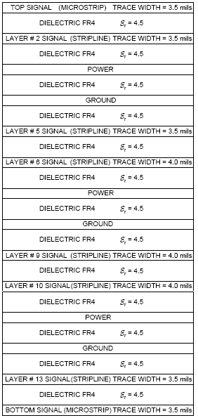
Figure 1 – PCB Layer Stack-up
Memory Interface Block Diagram
The memory interface scheme is shown in Figure 2.
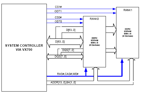
Figure 2 – DDR2 Interface Diagram
The scheme supports two ranks of memory, each rank containing eight 512Mbits (64M x 8) DDR2 memory devices. Total memory supported in the system is 1 Gbyte. As seen in the block diagram, the controller (VX700) address and control signal drives 16 receivers (inside memory devices). The topology for these signals should be carefully planned to avoid reflections. The data and DQS signals are easier to handle, as there are only three devices on these lines. Careful placement of memory devices will help the designer to achieve an efficient topology of both address/control and data/DQS bus. The memory chip placements and the bus topologies are described in subsequent sections.
Placement
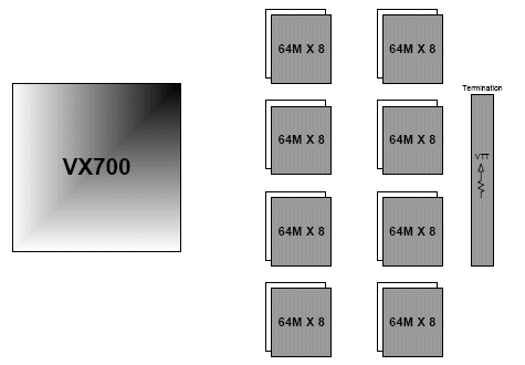
Figure 3 – Component Layout (Top & Bottom)
Figure 4 shows position of memory devices on the board with respect to the VX700 controller. Rank # 0 devices are placed on the top side of the board, while rank # 1 devices are placed on the bottom side.
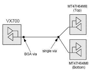
Figure 4 – Data Bus Topology
The DDR2 chips connected to same data lanes are placed in a clamshell fashion. Common vias are used to branch the data, data strobe, and data mask traces to top and bottom chips.
Data Bus Routing Topology
The data bus topology used in this design is straightforward and simple, as shown in Figure 5. This topology is applied to data lines D[63:0] and data strobes DQS[7:0]. These signals are routed with two vias, one near VX700 for BGA escaping, and the other near the memory BGA pads. The traces to the top and bottom memory BGA pads share the same via. The trace between the two vias is routed on some internal layer that is sandwiched between two continuous power planes (strip line geometry).
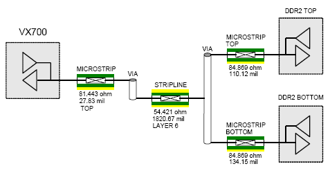
Figure 5 – Data Bus Simulation Topology
For simulation 75 ohms ODT (on-die termination) was selected (150 ohms // 150 ohms) on one of the DDR2 device (U42). Figure 7 shows simulation results for a write cycle at 266MHz. (DDR2-566). The waveform is probed at DDR2 BGA pad (U42).
The topology extracted from the routed board for one of the data line (longest trace) is shown in Figure 6. That diagram shows short traces on top and bottom layers (micro-strip) used to escape from the BGA areas.
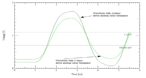
Figure 6 – DDR2 Data Write Simulation
The simulation produces better results with a 22 ohms series terminator, which can be enabled by software inside VX700. The simulation results for strobe signals DQS will be same, as same type of drivers & receivers are used.
Figure 7 shows simulation results for a read cycle at 266MHz. Here U42 is set as the driver and the internal parallel termination (150 ohms // 150 ohms) of U50 is enabled. The simulation probe is at U3 pin.
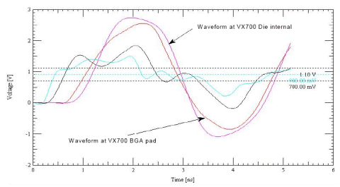
Figure 7 – DDR2 Data Read Simulation
Address Bus Routing Topology
The address topology used in this design is applicable to address lines ADDR[13:0], RAS#, CAS#, WE#, CS0#, CS1#, ODT0 & ODT1. The routing topology is selected based on the placement of the memory devices that will minimize the reflections and achieve proper setup and hold times with respect to clock. These signals are branched from a central point (via) to all the memory devices. The branches are symmetrical and length matched to achieve better signal quality.
The topology shown in Figure 8 is implemented for ADDR[13:0], BA[1:0], RAS#, CAS#, WE#. These signals are connected to all the sixteen DDR2 devices.
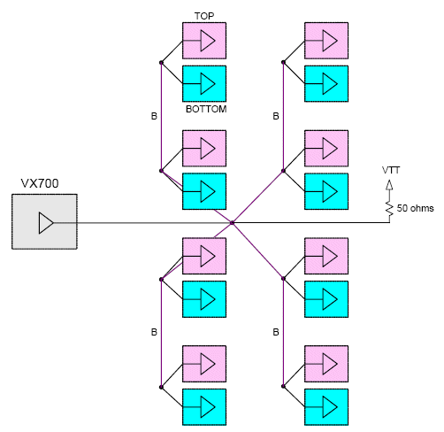
Figure 8 - Address Bus Topology
The dots represent vias on the PCB. As seen in the diagram, there is a central via positioned somewhere between the two rows of memory devices. This via makes a connection to branches (B) in a star fashion. Trace lengths of any of the branches (B) are matched. Notice that the termination resistor is hooked up to the same central via.
The topology extracted from the routed board (using Cadence signal integrity tools) is shown in Figure 9 for one of the address signal (ADDR2). Since there are sixteen receivers hooked to this signal, strongest driver was selected to run the simulation.

Figure 9 - Address Bus Simulation Topology
Notice that the long cylindrical via represents central via in the routing topology. Proper driver models are selected for VX700 address bus. Figure 10 shows simulation result at 133 MHz. (for DDR2-266) on this trace. The waveforms at all the DDR2 address receivers are superimposed to show uniformity at all inputs.
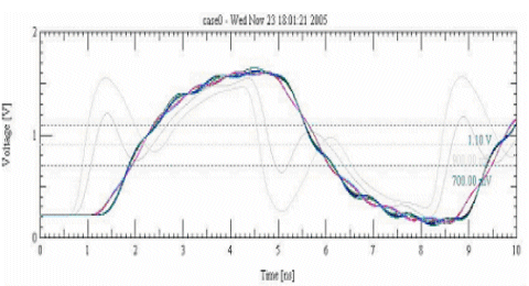
Figure 10 - ADDR2 Simulation Waveform
The waveforms in light color are at the driver internal (inside the die) and at the BGA pin. Notice that all the waveforms at the receiver have a fairly smooth transition and are not affected due to multiple reflections. This is due to the symmetrical topology and matched trace lengths adopted in the design.
It is interesting to note that the signal quality is not affected very much by the absence of the end termination (50 ohms). In especially tight board space instances, therefore, the designer can choose to avoid adding extra end terminations for address and control signals. Figure 11 shows simulation result on the same address line without the end termination. Notice that signal low level and the high level durations have reduced.
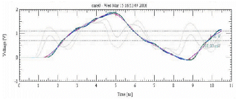
Figure 11 – ADDR2 Simulation Waveform without end Termination
In some cases, designers have to deal with very strong address drivers with sharp rising (lower rise time) and falling (low fall time) edges. This can affect the waveforms due to multiple reflections from nearer and further devices. A better way to address this situation is to add a low capacitor (10-22pF) very near the driver. This capacitor will work to increase the rise and fall times. Adding a 22pF capacitor right on the VX700 BGA via produces better simulation results as shown in Figure 12.
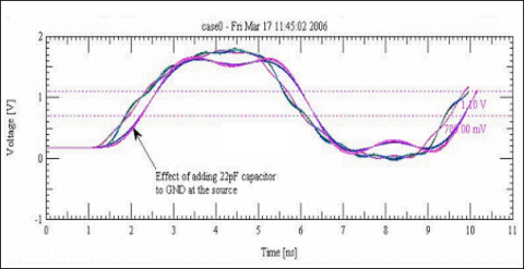
Figure 12 – ADDR2 Simulation Waveform with 22pF Capacitor at Source
This Figure compares to the results without the capacitor. There is a considerable improvement in the rising and falling edges at the receivers. There is a delay of almost 300 psec., which should not be a problem as long as the DDR2 clock edges are positioned properly. It is a good idea, therefore, to provide mounting options for capacitor arrays near the driver pins, if space permits.
Related Semiconductor IP
- DDR2 SDRAM Controller
- DDR and DDR2 SDRAM Controller Intel® FPGA IP Core
- DDR and DDR2 SDRAM Controller with ALTMEMPHY Intel® FPGA IP
- DDR2 Monitor Verification IP
- DDR2 Synthesizable Transactor
Related White Papers
- How to design 65nm FPGA DDR2 memory interfaces for signal integrity
- SOC: Submicron Issues -> Deep signal integrity can be assured
- Signal Integrity --> LVDS extends utility of 1149.1 boundary scan test
- Signal Integrity --> LVDS modeling techniques overcome Ibis inaccuracies
Latest White Papers
- Ramping Up Open-Source RISC-V Cores: Assessing the Energy Efficiency of Superscalar, Out-of-Order Execution
- Transition Fixes in 3nm Multi-Voltage SoC Design
- CXL Topology-Aware and Expander-Driven Prefetching: Unlocking SSD Performance
- Breaking the Memory Bandwidth Boundary. GDDR7 IP Design Challenges & Solutions
- Automating NoC Design to Tackle Rising SoC Complexity