Conquering the challenges of PCIe with NVMe in order to deliver highly competitive Enterprise PCIe SSD
Executive Summary: To help leading storage companies address the booming demand of PCI SSD (Solid State Drive), PLDA enhances the end-to-end data integrity functionality of its PCIe soft IP products and showcases a NVMe demo on its hardware.
PCIe, a key enabling technology in the Enterprise Solid State Drive Market
With an increase in popularity of Internet-based storage and cloud computing, the need to manage “big data” has resulted in a proliferation of server-based data storage farms. Within this segment, the need for speed and low latency is critical. The standard PCIe interface has emerged as an innovative and affordable solution for providing ultra-low latency and high data rates by enabling throughput of up to 6.6 Gb/sec, PCIe Gen 3 in an x8 configuration.
Today, with over 100 million enterprise PCIe ports on the market combined withrapidly growing offerings in term of port shapes and size, revenue forecasts for PCIe technology within the enterprise SSD Market are increasingly optimistic – a recent report suggests more than $2,000 M in Worldwide revenue in 2016. (Source : HGST - FlashMemory Summit 2013 Paper)
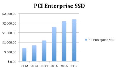
In this paper, we will describe the challenges PCI SSD providers face in order to launch the most competitive products in the Storage Enterprise Market. These challenges include:
- Creating an intrinsic end-to-end data protection capability that is transparent to the end users and a deliver a minimum impact on throughput and latency
- Providing a lower total cost of ownership and smaller carbon footprint
- Reducing production costs and time to market through interface standardization
Enabling end-to-end data integrity without impacting performance
Data integrity and data protection are key to providing a comprehensive solution to the storage market. SSDs always erase blocks before storing new information, and always use a newly erased block to store changed data, leaving the old data untouched in the old block. This technique is referred to as “wear levelling”. Because of this, address translation and data versioning techniques are essential to prevent the drive controller from returning stale data, e.g. data that was correct originally, but has since been updated.
To maintain performance, many flash vendors will perform the erase part of the cycle in advance and optimize performance with flash management features. A good way to enhance performance is to implement data integrity and data protection routines.
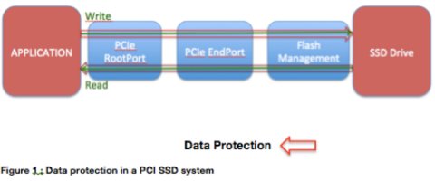
We can see in the Figure 1, at every juncture where data is transmitted, received, processed and stored, end-to-end data protection must perform data integrity checks. To be effective in the SSD system, this action must be processed in every device. At this level of throughput and latency, analog high-speed transceivers are highly sensitive, requiring an optimized and enhanced data protection system.
In order to address these issues specific to the storage market, PLDA has enhanced the native data protection functionalities of its PCIe IP products, enabling easier implementation of data protection strategies within the SSD.
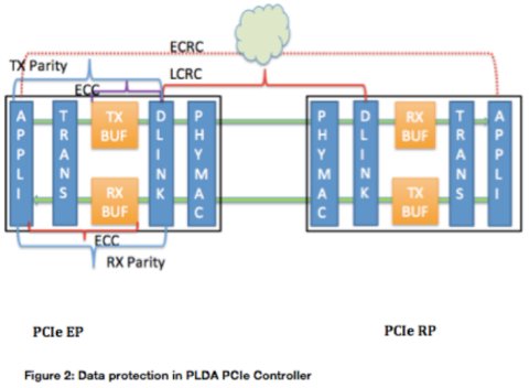
In the PLDA PCIe Controller, data integrity is ensured by a combination of several protections. They all play a unique role in preventing data corruption scenarios.
- LCRC protects the content of a Transaction Layer Packet (TLP) across a single PCIe link. It is generated and checked at data link layer level.
- ECRC protects the content of a TLP from its source to its ultimate receiver. It is generated and checked at transaction layer level or by application. Applications can generate or check it to ensure data integrity across the entire datapath.
- ECC is a mechanism present in some memory constructs that can detect and/or correct some data errors that occurred in the memory.
- Parity is provided to protect data between buffer and data source or consumer. A parity bit is added to each 8-bit or 32-bit block of data. These parity bits follow the same path as data until it is consumed.
- On the RX datapath: The data link layer generates parity and writes it with data to the RX buffer. Then parity is output on tl_rx_prot at the same time as data on tl_rx_data
- On the TX datapath : The application generates parity and provides it to the core on tl_tx_prot at the same time as data on tl_tx_data.
End-to-end Data Protection (ECRC, ECC, LCRC, Parity) has been enhanced on PLDA’s PCIe 3.0 soft IP portfolio as follows :
- PCIe 3.0 soft IP supporting endpoint, root port, dual-mode, switch and bridge configurations withadvanced features such as SR-IOV, multi-function, AER and more.
- Complete ARM SoC-optimized PCIe 3.0 soft IP supporting endpoint, rootport and dual-mode with configurable AMBA AXI3/AXI4 user interface including inbuilt configurable high-performance scatter gather DMA, address translation and ECAM support.
Bypassing the Host Processor - Options to further reduce latency and increase throughput
Typical storage controllers are composed of a communication interface and a NAND flash controller. In this scenario, all of the data flow is managed by the external host processor. The use of external processor architecture makes it difficult to manage high performance applications. Using an NVMe IP core is advised in order to off-load the use of a host CPU and is becoming a standard way to increase performance with minimal cost.
NVMe provides the following benefits:
- Ultra-low latency
- Very high throughput
- Low power architecture, delivering lower power consumption and resulting in a lower Total Cost of Ownership and reduced carbon footprint
- Reduced gate count
- Cost reduction and shorter time to market through use of a standardized interface
- Reliable performance across multiple cores enabling quick access to critical data
- An optimized register interface and command set that reduces CPU utilization resulting in higher performance and lower power
- Scalability with headroom for current and future NVM performance
- End-to-end data protection capabilities and support for standard security protocols, such as Trusted Computing Group
- Seamless integration into multiple operating system environments with standard open driver interfaces
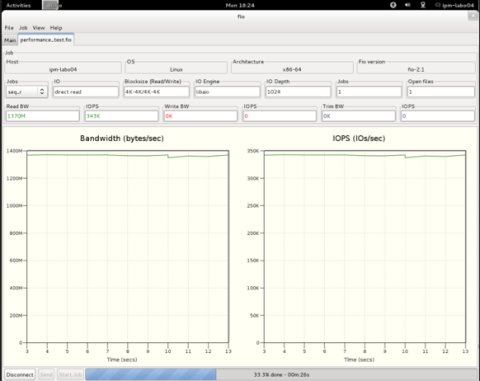
IP-Maker created a demo using PLDA’s XpressV7-LP PCIe-based FPGA board that demonstrated the incredible performance advantages of a full NVMe core.
- In this architecture, all commands and transfers are executed in hardware without any embedded CPU interactions
- The core directly addresses the cache memory (DDR3), with Physical address = Logical Block address
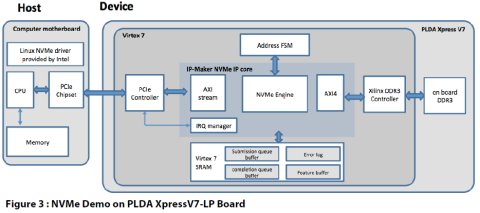
This scenario creates the following results:
- Measures on the FPGA-based reference design, Gen2 x4, using FIO
- 343 KIOPS Read (4kB)
- 270 KIOPS write (4kB)
- 12µs latency write (4kB)
- Scalable architecture
- 1MIOPS+ range for a Gen3 x8
How PHY optimization can reduce power consumption
For some time, reducing power consumption within a datacenter has become a prime goal in order to reduce costs and improve profitability. PLDA’s PHY partner, Global UniChip (GUC), oriented its PHY design to provide storage manufacturers the lowest power consumption. The GUC PHY, in addition to being fully BASE and CEM spec compliant, also supports features like SRIS (Separate Reference Independent SSC) and L1 PM Sub-states for storage applications.
L1 PM Sub-states is a feature that was added to PCIe specification several years ago in order to reduce power consumption. Historically, the PCIe link is widely held to consume too much power via leakage and through the Receiver Electrical idle detector circuitry. The L1 PM sub-states function addresses this through two sub-states - L1.1 and L1.2:
- L1.1 is used to maintain the common-mode voltage
- L1.2 turns off high-speed circuits.
PLDA and GUC together provide a fully integrated and silicon-proven solution for PCIe Gen3 with all the key features required for storage applications including L1 PM Sub-states, reducing power consumption without affecting performance.
Conclusion:
As the market for Enterprise SSD continues to grow, reliance on in-chip solutions to increase performance, reduce latency and optimize time-to-market will continue to be a focus. The use of innovative PCIe-based products such as IP products designed specifically for the SSD market will provide an optimal path to creating faster, cheaper and more reliable solutions.
Use of products such as the PLDA PCIe Gen 3 soft IP, GUC’s optimized PHY and IP-Maker’s NVMe core can provide:
- The lowest latency and best throughput figures available in PCIe SSD today
- Improved data integrity routines within the PCIe controller, eliminating the need for CPU power
- Optimized time-to-market and performance by utilization of standard interfaces
- Reduced footprint of the final chip through use of products designed to work together from the ground up
For more information on PLDA and its complete line of leading interface IP solutions, please visit www.plda.com.
About PLDA:
PLDA designs and sells intellectual property (IP) cores and prototyping tools for ASIC and FPGA that accelerate time-to-market for embedded electronic designers. They specialize in high-speed interface protocols and technologies such as PCIe and Ethernet. Visit them online at www.plda.com.
Related Semiconductor IP
- Universal NVM Express Controller (UNEX)
- NVM Express (NVMe) Controller (compliant with NVMe 1.4 Base Specification)
Related White Papers
- Advantages and Challenges of Designing with Multiple Inferencing Chips
- Revolutionizing Consumer Electronics with the power of AI Integration
- Handling the Challenges of Building HPC Systems We Need
- Streamlining SoC Integration With the Power of Automation
Latest White Papers
- Ramping Up Open-Source RISC-V Cores: Assessing the Energy Efficiency of Superscalar, Out-of-Order Execution
- Transition Fixes in 3nm Multi-Voltage SoC Design
- CXL Topology-Aware and Expander-Driven Prefetching: Unlocking SSD Performance
- Breaking the Memory Bandwidth Boundary. GDDR7 IP Design Challenges & Solutions
- Automating NoC Design to Tackle Rising SoC Complexity