Communication centric test and debug infrastructure for multi core SoC
Haridas Vilakathara, NXP Semiconductors
Abstract
A communication centric SoC debug approach using control transactions, as an extension of the traditional, processor based debug access and control is presented in this paper. A structured approach is presented to control both the processor core and other critical hardware units in a hardware synchronized manner, thereby enabling both synchronous stop and start during a debug session. An efficient and processor independent mechanism to have explicit control the system at run time is presented. The presentation also describes an efficient way to control the system through a tester/ATE
THE PROBLEM STATEMENT
The integration and debug of multiple cores, combined with an increasing ratio of overall gates vs. package IO, makes an increasingly dominant amount of a system design "“deeply embedded”, such that only minimal amount of data needed for analysis can be made available in real time at the chips pins. These deeply embedded systems introduce new analysis problems, due to the interaction and communications between multiple processor cores, and hardware IP units. The main focus of this paper is to describe a system level debug methodology that focuses on both the processor level interactions as well as the deeply embedded hardware transaction level communications.

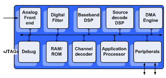
Figure 1 : Typical multi core SoC
Figure[1] shows a typical multi core software define platform SoC. As we can see the system may contain one or two DSP blocks and an application processor module as programmable processing elements along with a set of hardware accelerator unit and standard infrastructure and SoC peripherals. Such complex functionality and increased functionality demand that a high degree of integration be achieved in a single, compact chip (SoC). Real time response, high performance and at the same time lower power consumption are the typical challenges for any such SoC. Quite often such devices also use mixed signal technology to include many of the analog components along with the digital logic. The result is that, it becomes more and more difficult to verify and optimize such systems. Verifying such system at simulation level is time consuming, and some time impossible due to inaccurate validation models or test scenarios. This means more and more test vectors need to be exercised either by using a physical prototype or at silicon itself, where in it is easy to describe a real world test environment around the system.
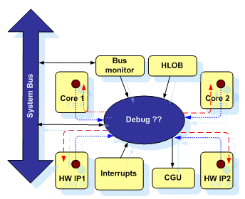
The basic debug problem: In a prototyping or silicon platform, the controllability and observability of the design is limited, primarily because of the following: a. increased complexity, b. deeply embedded logic, and c. the design is pad limited.

Figure 2 : The system level debug problem
System level debug problem: The problem of system level debug is further complicated by the fact that, in today’s typical SoC, the IP’s and processor cores may come from different IP groups, and third parties. Many of such IP’s may not have a standardized view towards system level debug. In summary we may state the following as key challenges towards a system level debug.
- Synchronization of processors from different vendors from a debug point of view is a challenge. Providing a hardware-aware debug solution is a greater challenge
- We need to focus on the communication between processor core’s and the underlying hardware infrastructure for an effective implementation of debug logic
The issue of test and measurement: Many of today’s SoC do contain greater amount of analog and mixed signal logic. In comparison with digital only logic test, the analog and mixed signal circuit test and measurement requires validation of extrinsic analog parameters. Traditionally this been achieved through analog BIST (built in self test) circuitry along with analog test bus. This imposes bigger limitation in the test and measurement space in terms of flexibility and the necessary circuit structures has to be in place along with the silicon. Here we may have to look for reusing the DSP present within the SoC to do such measurements, and in case if it is possible, how to communicate with the DSP for organizing the test and reading the test results in an efficient way. One another important factor to mentions is the reuse of test and debug infrastructure between test and debug group.

TEST AND DEBUG REQUIREMENTS:
Based on the problem statement above, the system level test and debug requirements can be classified under the following.
Software and application debug: Here part from the traditional individual processor based debug, many times we should have provisions for non-intrusive access to register and memory space during run time.
Break points: We should have provision to enter into a debug space either from a software event (software source level debugging) and hardware break points (enter into debug mode based on a hardware event such as, interrupts, bus transactions etc.)
Synchronized debugging: We should have provisions to enable synchronized debugging between processors. Further, it is desirable to not only synchronize processors during debug, but also SoC peripheral events generated such as timer events, hardware interrupts and bus transaction events. Here in principle we are looking for hardware transaction level communication events as a source for debugging. A synchronized stopping is quite easy to achieve, and almost all industry standard processor cores do support such features. However the problem of synchronized restart is bit tricky, and this may become specific to SoC, or do require proprietary solutions.
Silicon test and debug: Here we look for a standardized communication interface between the tester ATE (Automatic Test Equipment) and the SoC, so that the tester can control, load test vectors, and observe the results in an efficient way. Interface like JTAG may become the preferred interface.
Secure access: Many times the debug interface may be sued by hackers to gain access to the SoC and steal many intellectual properties, or alternative use of the SoC (e.g. Xbox used as cheap linux computer). Provision should be in place to avoid un authorized access to the SoC.
Performance monitoring: Many of the debug infrastructures, especially the hardware communication centric one may be used for analyzing the SoC performance during run time, and can be used to fine tune the SoC performance or power.
KEY CHALLENGES AND CONSTRAINTS
The following are the key challenges one have to solve while designing a system level approach towards debug.
Debug hardware: While designing a solution for the primary requirements stated in earlier session, one need to make sure that with respect to debugging alone, only minimum hardware real estate is used and no additional IC pins are used only for debugging. If the real estate for debugging is taking more than two to three percent of total IC real estate, then it become very difficult to sell the idea of debug to the system and IC architect.
Efficient debug access: Traditionally a JTAG interface is used as a debug access mechanism. Here there could be two ways of accessing the SoC resources. One is through the traditional processor debug port and second one is a have direct JTAG to system bus access. The second approach may be much more efficient in terms of access speed.
Synchronized debugging: The key challenge here is that in a typical SoC, the IP’s and processor cores may be coming from different sources, with or without a debug interface. Even if there is a debug interface, it may not be easy to integrate, because of interface mismatch. From a system level synchronized debugging point of view, here means stop all processors on an SoC in case a debug event occurs on one of them, and starting them at the same time again when all involved debuggers have finished debugging. Synchronized stopping of processor core is not an issue. However synchronized restart is complex and may need special attention. Apart from this halting critical hardware IP/modules under debug context may require a centralized debug communication within chip to take care of clock level granularity requirement for such actions and for clock domain synchronization to avoid any race conditions.
Test and measurement: In order to have an efficient control over system infrastructure and processor core, it may be necessary to have full control over the system start up control, so that the ATE can control and initialize the processor core or the DSP.
APPROACH TO THE PROBLEM
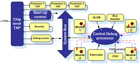
In this paper a hardware communication centric SoC debug approach using control transactions is presented, as an extension of the traditional, computation-centric debug approach. In this approach, the complete system can be monitored and breakpoints can be set on the progress of both processor level interactions and communication tasks originating from CPU/DSPs, IP’s or the bus infrastructure. This is achieved by observing the running system through centralized debug processor module. The breakpoints from both processor core and hardware IP’ are centrally collected and redistributed to a (subset of) core(s) to halt or stop the system. After a breakpoint hit, the bus infrastructure no longer accepts data from the master/initiator side, and force the system to enter into functionally idle state. In this state it is safe to apply a JTAG core-based scan method to obtain state information. After obtaining state information, the renewed acceptance of commands and delivery of data from and to the masters and slaves can be controlled from an external debugger tool.

Figure 3 : Approach to system level debug
The key innovative attributes of the approach are following
- Synchronous start and stop of processor core(s) and hardware IP’s
- Hardware transaction level debug: For multi-cycle operations such as on chip buses, with some signals in a bus cycle becoming active at different times, debug should take the form of sequential trace, rather than as a single-cycle snapshot. This solved by adding debug logic to monitor bus transactions.
- System level control during debug: Operational problems are often interrelated with the operations of at multiple communicating blocks (a processor and memory peripheral as an example). Here in a debug context, we should have provision to halt the execution of all such communication blocks (including hardware IP units) to preserve the system state information
- Break points can be set by monitoring hardware IP states or bus conditions in addition to conventional program counter based approach
- Extension of chip level TAP to for easy integration with external debug tools as well as DFT tools
- Can be used by a tester (ATE) for efficient access to system components, along with explicit system start up control
- Concept can be extended to aid performance monitoring and adaptation
- Very less area overhead by reusing part of DFT infrastructure for implementation
- Completely secure by adding specific security engine into JTAG access path
- No interface/functional changes to the IP/bus infra to adopt the debug concept
The section below will explain the important implementation aspects we have taken care during the design
Hardware synchronized debugging: Here a centralized cross-trigger facility has been realized as part of the central debug processor. Full programmability of the cross trigger matrix is possible through a programming interface that is accessible through the JTAG-System bus- Central debug processor hardware interface. Facility exists for collecting break points from both processor initiated debug events as well as for the entire hardware state event monitored within the central debug server. The cross triggering action is explained through an example below

Figure 4: Cross trigger unit
| Condition | Action |
| Entry condition for debug | Hardware or software debug event |
| Debug action (synchronous stop) | Stop or halt processing elements ; Stop: Processor enters debug mode; Halt: Processor is halted ( stop clock for example); HW units: Stop clock or assert debug event ( if IP support a debug halt input) |
| Exit condition (synchronous start) | By monitoring the debug state of the source and processor state. Also through explicit communication through debug control software |
Figure 5 : Cross trigger example
| Event no | Action |
| 1 | P1 enters debug mode( SW event) |
| 2 | P2 stopped (HW event) |
| 3 | P2 enters debug mode (debugger notified) |
| 4 | P1 exits debug mode (SW event) |
| 5 | P1 continues in halt mode & P2 still in debug mode |
| 6 | P2 exits debug mode |
| 7 | Both processor continue execution |
DSP BASED TEST INFRASTRUCTURE
The idea of using DSP for AMS circuit testing is already exits, and many literatures available for efficient algorithms to do such test across various AMS circuits. One of the critical issues so far was the speed and capabilities of on board DSP to accomplish such test in affordable time. Today’s many multi cores SoC platform do have very powerful processor that can effectively bridge this gap. The following are the typical questions that get answered by using a DSP based test and measurement approach
- AMS testing requires extrinsic parameters validation. DSP in loop testing can effectively fulfill this requirement
- Many AMS modules provide trimming capabilities to fine tune performance. This means the AMS circuit may need to be tested at boundaries and across various operational conditions. We may have to test these settings before declaring pass/fail
- DSP offer better flexibility and faster when doing multiple measurements (reducing test set up time). Hence may be considered as an effective replacement
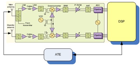
The figure[6] below explains the basic infrastructure required to enable such DSP based test and measurement of AMS circuits. If the AMS circuits offer both transmit and receive (e.g. DAC & ADC pair) functions, then the ATE need to communicate only through the JTAG interface. Using the debug infrastructure the ATE can control the DSP core, initialize the DSP memory with a test program, then excite the DSP to do a loop back testing involving the AMS unit, followed with a result query to the DSP. If the AM circuit offer only receive function (only ADC for example) then the analog input test waveform need to be supplied by the ATE itself.
Figure 6: Test and measurement support
PERFORMACE MONITORING AND CONTROL
A communication centric debug infrastructure provides much facility for closely monitoring the hardware transactions and features for controlling the same. Similarly there are many test specific features in a SoC that could be useful for analyzing the performance of the system. This can be effectively used for performance monitoring and adaptation at system level.
The performance monitoring actions can be categorized into three major activities. Observe Analyze and control. These are explained in below table
Figure 7: Performance monitoring and control
The observe actions is primarily concentrated on observing the key hardware transactions, silicon operational parameters, and the application profile by reusing the design for debug infrastructure and test infrastructure.
| Action | Observe |
| Bus transaction | By observing system bus transaction, we can identify the system bus utilization, BW utilization or access latency with respect to the transaction originating units. Another important parameter is the bus contentions or conflict between different modules in sharing the shared bus infrastructure. |
| Process monitor | A process monitor is a typical test related unit used by the test engineers to identify and measure semiconductor process related information. A typical process monitor unit will help in identifying the process corner of the chip, temperature and other process performance related parameters. |
| System work load estimator | This may not be a debug or test related infrastructure. This may be a central unit added specifically for performance measurements. This unit may work in conjunction with the system software to identify the application related performance requirement of the underlying hardware |
The analysis action can be done either offline or at run time. The run time analysis is more attractive from a performance management view point. However this may require additional processing power form one of the central processor, along with a centralized dedicated hardware unit, where all information is present from the respective observation units.
| Action | Analyse |
| Bus transaction | Analyse the effective utilization of the shared system infrastructure such as system bus |
| Process monitor | Identify the semiconductor process corner at which the chip is working. A Fast-fast corner may work at improved speed, and slow-slow corner may not |
| System work load estimator | Estimate the load on the processor, and MIPS requirement based on application demand. This can be static, where in the information may be simple look up table based, where in the control software will set the basic performance requirement of the underlying hardware based on application load. A dynamic adjustment of the hardware parameters also possible with tight close loop control between hardware elements and underlying software |
The control actions in short can be classified into three groups.
- Dynamic frequency scaling: Adjust the operational frequency of the whole chip or processing islands based on the performance requirement.
- Adaptive body biasing: Here both forward biasing and reverse body bias techniques can be used to achieve required performance objectives, without the need to varying the SoC core voltage.
- Adaptive voltage scaling: Adjust the core voltage either at global SoC lever or local level (voltage islands) to achieve the desired performance requirement.
| Action | Control |
| Bus transaction | Based on the measured load on the shared infrastructure, the control module may decide the operational frequency of the bus infrastructure network. A simple algorithm may set 70% bus utilization at any given point in time irrespective of the application load. Need closed loop control. |
| Process monitor | Once you know the underlying hardware physical profile and operational conditions, the same can be compensated either by increasing or decreasing the operational parameters such as adaptive voltage scaling, and adaptive body biasing. A reverse body bias can be applied at entire SoC level (reduce leakage when standby) , and a forward body bias can be applied at select portion of the chip (for better speed performance at the expense of more leakage current) |
| System work load estimator | A system work load estimator can be used to fine tune the chip operational parameters based on the application work load. Can be a simple look up table based or truly can be a run time closed loop system. The later may require additional logic plus processing power. Based on the requirement, we may apply dynamic frequency scaling, adaptive voltage scaling or adaptive body biasing, or a combination of all. |
CONCLUSION
To analyze problems and optimize performance in multi-core operations, the designer should be able to exercise any and all core debug features and interfaces through them.
To address system level debugging, a hardware transaction level debug controller is presented as a debug triggering environment supporting multiple on-core and inter-core conditions and global actions to all or a subset of the cores on an SoC.
Since Complex systems communicate over a range of buses, it is important to be able to monitor signals on the embedded buses, and to trigger on and trace bus operations based on specific conditions
The debug environment described above is reusable for similar SoC platforms. This is primarily because of the standardized debug communication channel & centralized debug topology
The debug environment can be extended to next level performance monitoring and control
REFERENCE
[1]Transaction-based communication-centric debug”, Kees Goossens, Bart Vermeulen, Remco van Steeden, Martijn Bennebroek, NXP Semiconductors
[2] Performance Monitor Unit Design for an AXI-based Multi-Core SoC Platform, Hyun-min Kyung, Gi-ho Park, Jong Wook Kwak, WooKyeong Jeong, Tae-Jin Kim, Sung-Bae Park
[3] System awareness improves SOC power management, Satish Sathe, Senior Systems Architect, Applied Micro Circuits Corp.
[4] Intelligent Energy Management for Portable Embedded Systems, Krisztian Flautner and Dipesh I. Patel, ARM Limited
[5] DSP-Based Testing of Analog and Mixed-Signal Circuits, Matthew Mahoney, ISBN: 978-0-8186-0785-1
Related Semiconductor IP
- NPU IP Core for Mobile
- NPU IP Core for Edge
- Specialized Video Processing NPU IP
- HYPERBUS™ Memory Controller
- AV1 Video Encoder IP
Related White Papers
- Reusable debug infrastructure in multi core SoC : Embedded WiFi case study
- Design and Implementation of Test Infrastructure for Higher Parallel Wafer Level Testing of System-on-Chip
- Optimizing Communication and Data Sharing in Multi-Core SoC Designs
- A RISC-V Multicore and GPU SoC Platform with a Qualifiable Software Stack for Safety Critical Systems
Latest White Papers
- Ramping Up Open-Source RISC-V Cores: Assessing the Energy Efficiency of Superscalar, Out-of-Order Execution
- Transition Fixes in 3nm Multi-Voltage SoC Design
- CXL Topology-Aware and Expander-Driven Prefetching: Unlocking SSD Performance
- Breaking the Memory Bandwidth Boundary. GDDR7 IP Design Challenges & Solutions
- Automating NoC Design to Tackle Rising SoC Complexity