Reusable debug infrastructure in multi core SoC : Embedded WiFi case study
Bangalore India
Abstract:
With increase in hardware and software content in today’s complex SoC, it becomes a necessity to verify such system from a system viewpoint. Providing a means to effectively debug such systems from a system perspective is vital in help to pin point the problem and thereby reduce the number of chip re-spin. This paper outlines a system level reusable hardware-software debug infrastructure for a complex multi core SoC and describes how this can be integrated with existing third party debug tools such as ARM MultiIce and logic analyzers. The concepts are illustrated through the case study of multi core multi million gate embedded WiFi project. This approach provides a "debug backplane" to address dense and complex multi-core systems analysis, such as processor behavior, embedded logic block functions and deeply embedded bus traffic.
1. Introduction
Large complex applications and increased functionality demand that a high degree of integration be achieved in a single, compact chip (SoC). Real time response, high performance and at the same time lower power consumption are the typical challenges for any such SoC. Quite often such devices also use mixed signal technology to include many of the analog components along with the digital logic. The result is that, it becomes moer and more difficult to verify and optimize such systems. Verifying such system at simulation level is time consuming, and some time impossible due to inaccurate validation models or test scenarios. This means more and more test vectors need to be exercised either by using a physical prototype or test silicon, where in it is easy to describe a real world test environment around the system. However in a prototyping or test silicon platform, the controllability and observebility of the design is limited, primarily because of the following: a. increased complexity, b. deeply embedded logic, and c. the design is pad limited.
The observation of critical control signals is an important aspect of system verification and to a great extent this does exist in the software part of system verification flow by using standard software debugs tools. In hardware portion of the system it is very difficult to observe internal signals primarily because of the external pin count limitations. A number of methods have been used to facilitate this obeservability issues. Few of them are listed below.
- ICE based verification for SW
- Multi core debugging
- Hardware monitors
- Synthesizable assertions
- Reuse of DFT
In this paper a system level debug infrastructure is presented, taking advantage of the methods described above. The reuse of DFT is not really experimented and this is kept as a future extension for this project. The concepts are illustrated with an embedded WiFi SoC design.
2. Embedded WiFi
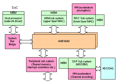
Fig 1: Embedded WiFi block diagram
Figure [1] shows the overall architecture of the embedded WiFi IP. The core system consists of following major blocks.
-
Host processor (ARM920T) sub system is responsible for the network layer protocol.
-
An ARM (ARM7TDMI) subsystem responsible for non real time MAC protocol as well as interfacing with application processor.
-
A RISC subsystem along with few hardware accelerator module for real time MAC protocol
-
A DSP subsystem along with hardware accelerators and analog module for MODEM functionality.
-
A peripheral subsystem for external communication.
3. The debug Requirement
As is typical in the wireless industry, this IP uses both general-purpose CPUs and a dedicated DSP core in order to achieve both software programmability as well as specialization. The modules are connected together by using AHB multilayer bus matrix.
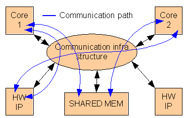
Fig 2: Control and data communication
The data and control communication within the system is organized through communication infrastructure. With the complex interactions of multiple processors and peripherals, there are many communication links that require deep observation and debugging in order to ensure that high-quality system is delivered. For a design relying heavily on synchronization through memory as well a high speed data bus matrix, as is the case with the system in Fig[2] is prone to synchronization problems (between processor, memory access, h/w accelerator utilization), The typical problems that can occur at the system level can be of the following nature
| Area of concern | Typical problems |
| Shared memory access | Data corruption Race conditions |
| Inter processor communication | Deadlocks Stalls |
| Processor performance | Starvation |
| System bus | Congestion |
| Peripheral performance | Latency |
Based on the statement above, the following are treated as the top level requirement for a system level debug infrastructure.
Controllability: The system here contains few programmable processor cores as well as dedicated HW IP modules. The individual processor cores provide software level controllability at individual core level (e.g. ARM MultiICE) through their debug extension. However these kind of traditional processor debug extension can provide only a snapshot from individual core perspective. However at an integrated level this is not sufficient primarily because the processor itself is deeply embedded in the system. Also deeply embedded system introduce new problem due to the communication between processor cores.
Observability: The system level observability is low, primarily because highest levels of hardware and software integration into the SoC and at the same time the functional I/O pins available for the SoC are limited in number. Also as these processor cores share the system resources, their dynamics and the interaction at system level are very difficult to observe by using traditional debug solutions.
| System level observabilty issues |
|
Access to individual module debug environment
: The system contains few programmable processor cores along with their own software debug environments. The designer should be able to exercise all or all the core debug features and interfaces through them.
Provision for system level debug: The debug infrastructure must also support the observation of signal at the system level. This means the debug environment need to support multiple on-core and inter-core conditions (breakpoints, trace points, other specific control or status conditions) and send global actions to all or a subset of the cores (halt/stop processor cores, clock gating to HW IP modules, interrupts etc.).
Hardware aware debug: The system described above contains lots of HW IP interacting with the programmable processor core. Monitoring the interaction between these modules is vital in isolating system level issues. From a debug perspective this means that, a hardware event can push the system to a debug state. Similarly software also can put an IP into debug state without halting rest of the system.
Debug synchronisation: Systems level debug must address blocks running over several clock domains. Robust approaches to global timestamp synchronization are needed to support coherency between multiple debug environments that may be involved for different cores on a single chip.
Scalability: The debug infrastructure must be scalable in the sense that with minimal additional internal wiring and with no increase in external I/O it must be possible to add additional modules and their debug extensions into the debug framework.
Reusability: Cores or IP with built in debug functionality will be reused in multiple designs. The debug interface as well as functionality must be reusable at any levels of system integration. Modular approach with standardized debug interface is highly recommended here. For example the SoC described in this paper can become a sub system in a larger SoC. We should be able to integrate the debug framework into the larger SoC platform with minimal integration effort.
4. Approach
Fig shows the baseline architecture of the debug frame work.
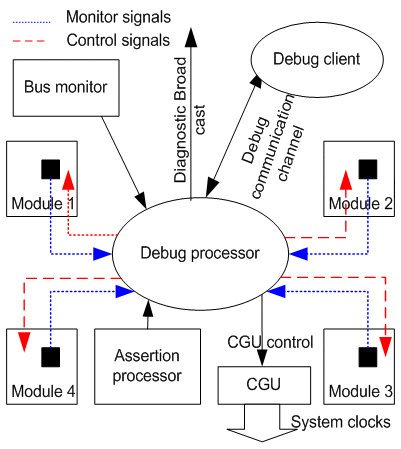
Fig 3: System level debug approach
The heart of the system is the debug processor itself, which is used to monitor and control the internal modules of the system. The debug processor is connected to the external world through a debug communication channel. In addition the programmable processors in the system can communicate with the debug processor through the internal bus, thus providing additional flexibility. System level observability is achieved by integrating the following debug modules to the debug processor in addition to the monitored signals.
-
Bus monitor
-
Assertion processor
-
Debug communication channel
-
Debug client
Bus monitor: The communication infrastructure defined in fig[3] is realized by using AHB MLM. The bus monitor provides a facility to monitor and trace all master transactions happening on the AHB MLM bus matrix. The bus monitor can be configured to capture the traffic over specified address and data range. An arbitration scheme also employed here, that will enable to capture data traffic in an optimized manner (round robin, arbiter locked to particular master etc). This enable to capture inter related data transfer over the MLM. As an example, it is very unlikely that a write and read can happen simultaneously from a single master to a memory connected to MLM. However write from one master and read from another can happen simultaneously. Here the bus monitor can be configured to capture all write transaction from one master and read transactions from another one. This kind of configurability will significantly reduce the amount of useful data that need to be traced and managed.
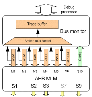
Fig 4 System bus monitor
Debug processor: Support for software level debug exists in many of today’s software development environments. Typical RTOS development environment can provide information about task-scheduling events, inter-process communication, synchronization, resource utilization (CPUs load, semaphores, I/O), external interrupts, etc. However this is done through additional software probe code, and when removed can affect the system timing behavior. One way to avoid this is to monitor the HW/SW events in a intrusive way. This can be done through an addition of logic at RTL level. Such hardware based monitoring system makes the SoC observable and work as a probe as well as debug trigger for both hardware and software. Typical probe events are: a. certain events on communication infrastructure (address data or control events); b. interrupts assertion; c. specific events/flag in HW IP.
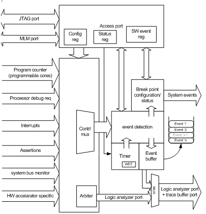
Fig 5: Debug processor.
Software also can generate events by writing through the software event register. The event detector performs a data comparison on the input event against what is configured in the configuration registers (e.g. a particular address access on MLM port), and once the event has occurred, the event is moved to the event buffer along with a time stamp. The time stamp is taken from a programmable (time granularity can be configured) timer. The timer provides the relative system time for the event. There is a provision to re route the events to external RAM for long-term event analysis. The monitor logic is connected to the internal system bus as well as to the external debug communication channel, making it possible for the processor /external debug controller to access the probed data. A watchdog timer also included in side the timer module.
Logic analysis (diagnostic broadcast): The monitored signals at the debug processor are put across to the logic analyzer through an arbiter/control unit. This is primarily because of the limitations in Primary I/O. The monitor signals are grouped into 4 channels. In any channel, there is a possibility to select any one of the monitor signal group. The channel information can be muxed to the O/P logic analyzer port in a time-multiplexed manner. The O/P information can be distinguished by using a frame start signal. The use of Diagnostic Broadcast is to provide support for logic analyzer based debug. Diagnostic Broadcast makes information about the state of the internal system available to the external environment, without compromising the performance of the system. Broadcast information can be viewed using a logic analyzer. The state capabilities of the logic analyzer can be used to view information about the transactions in progress on the bus. When coupled with an inverse Assembler for the processor it becomes a powerful debugging tool, providing a real-time trace of the instructions executed over the past few cycles. The trace can be triggered in several different ways (e.g., on specific addresses, data values, or particular control signals.) This provides a very flexible way to trap and analyze a given event or circumstance. Data transmission to the external environment is via a diagnostic bus.
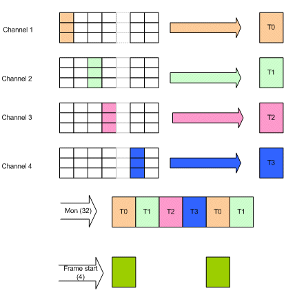
Fig 6: Diagnostic broadcast
System break point generation: Any one of the selected events can be used for creating a system break point (break point to each processor). The break point can be generated either by individual bit field or by a group of signals. Some examples are
- Any of the monitor signal
- MLM access (master) over a specified address range (inside address range or outside address range)
- AHB bus access error.
- DMA engine status
- Hardware accelerator status
- Signals from assertion processor
- Software breakpoints (configuration register)
The generated system break points can be used to send either global debug actions to different modules or local debug actions. This can be configured through the debug client. Typical debug actions are halt/stop to processor cores, clock gating to HW IP modules or may be a debug interrupt. The system break point status is available in the status register space, and this is communicated to the debug client.
Clock control: The debug processor is connected to the central clock generation unit. There is a possibility to configure this through the configuration interface. This facility will allow stopping hardware from a software-generated event. The processor core does not enter into a debug state. The software monitors the HW IP through its register interface. When a particular behavior is detected, then the processor can command the debug controller module to stop clock to the IP or put the IP in a halt state. The processor can then examine the system behavior (check buffer, reg IF etc.)
Debug communication channel: Traditionally single processor systems come with either a JTAG interface or a debug UART interface so that debugging is possible at the software level. The JTAG interface is used for debug communication primarily because of reduced pin count. With multiple cores or functional blocks, there are two possibilities to connect the system through a JTAG port.
The first option is to have a JTAG interface for each module (parallel JTAG) and this provides better controllability, and enables concurrent access to the individual modules. However the biggest problem is the increase in the pin count and scalability (when a new module added additional JTAG port to be added). The other option is to have a daisy chained JTAG approach and this is followed in this project. The primary reason to choose this approach is to reduce the I/O pin requirement (only one JTAG). Also, later if required additional modules can be interfaced to the debug chain without increase in external pins (scalability). One of the major bottlenecks in using such an approach is that concurrent access to different processing elements is not possible, and this introduces high latency in synchronized debugging. However through tools like ARM MultiICE, this can get interfaced with individual core debuggers and the latency can be taken care by adding additional hardware inside the SoC (HW synchronizer). The scheme is shown below.
The scheme presented in fig[7]. Supports for multi core debugging with tight synchronization is made possible here through a target synchronizer. Here the hardware synchronization module can be pre-programmed to control the target hardware.
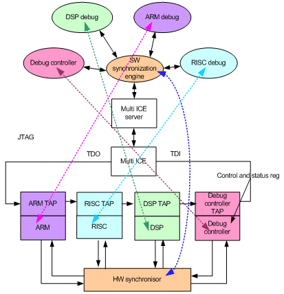
Figure 7: Debug communication channel
For example when a break point is hit in the ARM, the same information is captured by the target synchronizer, and the target synchronizer is programmed to halt the other two processors (either a debug interrupt is generated or clock to the processor module is stopped). The hardware synchronizer also captures the debug status of the processor. This in turn is communicated to the software synchronizer module, and the respective debug software module is informed. The matrix implementation can also take care of any race conditions arising out of cross triggering (for example DSP and RISC stopping each other and getting into a dead lock situation).
Debug client: This is the software portion of the debug controller. This module communicates with the debug processor over the JTAG interface. This module is used for the following purpose
- Configuring/controlling the debug processor
- Capturing the debug data
Assertion processor: Typically HDL designer can enjoy white box verification benefit at system level by including assertion checks in the HDL code they generate. In relating to HDL code, “assertion checks†are often referred to as “watchdog logicâ€. Here no real hardware logic is intended to be built and the “watchdog logic†is only intended to be used during RTL simulation. However some of the logic used here may be useful during a physical prototype level verification or even in actual silicon and this can tell us whether the control and data flow in the module is working as expected
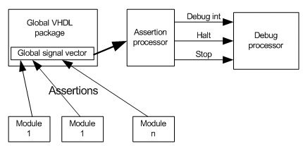
Fig 8: Assertion processor
Here we look for a way to synthesize simple assertions, and during system level verification, these can act as trigger points to enable debugging. A simple way to do this is to create a global signal variable (vector) that gets asserted when assertions are occurring. This signal vector can be trapped into the debug controller frame work as trigger points. Typically assertions can be of varying severity (note, warning, and error). So before passing the assertion to the debug processor, the assertions are filtered by an assertion processor. The assertion processor implemented here is a simple priority encoder along with a counter. Depending on the severity the assertion processor can initiate necessary debug actions.
5. Summary
The need for more advanced debug solutions is arriving rapidly. While many point solutions for debugging of individual processors or IP subsystems have been developed, the focus is now moving to the system level. As this debug scope increases, the responsibility for debug solutions moves from the processor developer (interested foremost in the debug of their own core) to the system developer with a core and architecture independent focus on diagnostics and analysis of the whole system and all its components. A system level debug approach is presented in this paper and this approach provides a "debug backplane" to address dense and complex multi-core systems analysis. By using instrumentation blocks as resources for "embedded intelligent" debug operations, analysis features such as system wide error recognition and filtering, and cross triggering between different subsystems of a complex architecture are supported. The baseline environment addresses four major facets of the system level debug problem:
-
The need to concurrently access debugs extension of all the programmable cores in a system. To analyze problems and optimize performance in multi-core operations, the designer should be able to exercise any and all core debug features and interfaces through them.
-
To address system level triggering, a hardware debug controller is presented as a debug triggering environment supporting multiple on-core and inter-core conditions and global actions to all or a subset of the cores on an SoC.
-
Since Complex systems communicate over a range of buses, it is important to be able to monitor signals on the embedded buses, and to trigger on and trace bus operations based on specific conditions.
-
The debug environment described above is scalable and reusable for similar SoC platforms. This is primarily because of the standardized debug communication channel (JTAG based) and monitoring and triggering is done at system level by integrating the individual module level instrumentation.
6. Acknowledgment
A large part of the embedded WiFi design including the debug framework is reused from an existing NXP internal WiFi solution form our wifi competence centre situated at Dresden Germany.
Reference
[1] A. Berent. Debugging Techniques for Embedded Systems using Real-Time Software Trace.
http://www.arm.com/pdfs/CoresightWhitepaper.pdf
[2] The ARM7TDMI Debug Architecture, Document No. ARM DAI 0028A, December 1995, ARM Ltd.
[3] ARM RM Target Integration Guide, Document No. ARM DUI 0142A, December 2000, ARM Ltd.
[4]Multi-Core Embedded Debug for Structured ASIC Systems, Dr. Neal Stollon,Rick Leatherman, DesignCon 2004
[5] Debug and Diagnosis in the Age of System-on-a-Chip, Robert Molyneaux, Sun Microsystems Inc.
Related Semiconductor IP
- Wi-Fi 7(be) RF Transceiver IP in TSMC 22nm
- Wi-Fi 6 (ax)+BLEv5.4+15.4 Dual Band RF IP for High-End Applications.
- Wi-Fi 802.11 ax/Wi-Fi 6 /Bluetooth LE v5.4/15.4-2.4GHz RF Transceiver IP for IOT Application in TSMC22 ULL
- IEEE 802.11n/ac/ax (WiFi) LDPC Decoder and Encoder
- WIFI 2.4G/5G Low Power Wakeup Radio IP
Related White Papers
- Challenges in developing a reusable IP core USB OTG IP case study
- Communication centric test and debug infrastructure for multi core SoC
- IP Processor Core Platform Selection According to SoC Architecture: a case study
- SOC Stability in a Small Package
Latest White Papers
- Ramping Up Open-Source RISC-V Cores: Assessing the Energy Efficiency of Superscalar, Out-of-Order Execution
- Transition Fixes in 3nm Multi-Voltage SoC Design
- CXL Topology-Aware and Expander-Driven Prefetching: Unlocking SSD Performance
- Breaking the Memory Bandwidth Boundary. GDDR7 IP Design Challenges & Solutions
- Automating NoC Design to Tackle Rising SoC Complexity