Comparing AMBA AHB to AXI Bus using System Modeling
By Deepak Shankar, Mirabilis Design
Embedded system designers have a choice of using a shared or point-to-point bus in their designs. Typically, an embedded design will have a general purpose processor, cache, SDRAM, DMA port, and Bridge port to a slower I/O bus, such as the Advanced Microcontroller Bus Architecture (AMBA) Advanced Peripheral Bus (APB). In addition, there might be a port to a DSP processor, or hardware accelerator, common with the increased use of video in many applications. As chip-level device geometries become smaller and smaller, more and more functionality can be added without the concomitant increase in power and cost per die as seen in prior generations. System Modeling is a new methodology above the detailed chip implementation level that allows one to explore different designs without having to write Verilog, System Verilog, VHDL, SystemC, or just plain C/C++ code. This saves considerable development time, and allows for more design exploration prior to selecting a design topology to begin implementation. This paper discusses the construction of an AMBA Advanced High-performance Bus (AHB) Shared Bus and AMBA Advanced eXtensible Interface (AXI) point-to-point Bus using a graphical modeling environment that achieved approximately 95% cycle accuracy. The graphical model and simulation analysis was completed in approximately one week.
To make the evaluation of the two busses comparable in terms of flow, throughput and latency, the following considerations were adopted:
- The AHB is a single-channel, shared bus. The AXI is a multi-channel, read/write optimized bus. Each bus master, or requesting bus port, connects to the single-channel shared bus in the AHB, while each AXI bus master connects to a Read address channel, Read data channel, Write address channel, Write data channel, and Write response channel. The primary throughput channels for the AXI are the Read/Write data channels, while the address, response channels are to improve pipelining of multiple requests. Assume there are four masters on each bus going to three slaves. The four master ports might include uProcessor, Direct Memory Access (DMA), DSP, USB. The three slaves might include on-chip RAM, off-chip SDRAM, and an APB bus bridge.
- To approximate the bandwidth of the two busses, one must count the number of read/write channels of the AXI Bus – six for three bus slaves. This suggests that the AHB Bus should support some multiple of bus width and/or speed to match the data throughput. The System Model can vary these combinations with simple parameter changes, however, the AHB bus speed was assumed to be double the AXI Bus, and two times the width. This will make the comparison of the two busses more realistic.
- To evaluate the efficiency of both busses, different burst sizes were selected; small, medium, and large. Small equates to the width of the AHB Bus, medium equates to two AHB Bus transfers, and large equates to four AHB bus transfers.
- If the AXI is a 64 bit bus running at 200 MHz, then the AHB will be a 128 bit bus running at 400 MHz. The burst sizes will be: small (16 Bytes), medium (32 Bytes), and large (64 Bytes).
This paper will focus on the requirements for quick model construction, the attributes to be monitored and workloads to be generated. The design goal is to select the bus that performs best in terms of throughput, latency, and utilization for single or multiple channels. The analysis will compare the two bus technologies side by side for 16, 32, and 64 Byte transfers. Average per channel utilization relates to power consumption. While the AXI Bus has multiple read/write channels to improve performance, and should perform better on average and peak latency measurements; it is not clear by how much due to the concurrency of internal bus transfers. The shared AHB Bus should be utilized more efficiently; it is not clear by how much due to the arbitration algorithm. The System Level Model will provide insights into to both busses, such that a designer could select the right bus for a particular application.
For this modeling exercise, we used standard system design and exploration software called VisualSim from Mirabilis Design Inc. This is a concept engineering software application that enables rapid exploration of embedded systems for performance and power trade-off. We could create models in this graphical environment using the configurable, parameterized library blocks, application-specific functions, standard component generators (processors, memory, caches, bus and switches) and a template-driven SystemC. The simulation environment optimizes the initial concept through a series of modeling refinements and abstractions to allow the best architecture to become an executable specification.
System Model Overview
The AHB Bus Comparison Model is shown in Figure 2 and the AXI Bus Comparison Model is shown in Figure 3. The system model consists of the following:
- uProcessor, DMA, DSP, and USB Master bus ports.
- AHB or AXI Bus Arbiter.
- RAM, SDRAM, and Bridge Slave bus ports.
- Result plots and window displays for statistics.
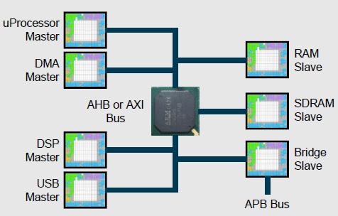
Figure 1: Block Diagram of the Bus Comparison Model
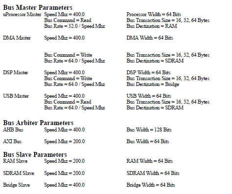
Table 1: Parameters of the simulation study between AMBA AHB and AMBA AXI
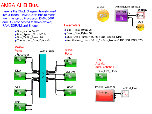
Figure 2: Block Diagram of the AHB Bus Comparison Model
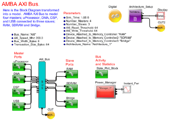
Figure 3: Block Diagram of the AXI Bus Comparison Model
Modeling Results
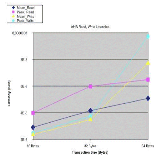
Figure 4a: AHB Read/Write Latencies
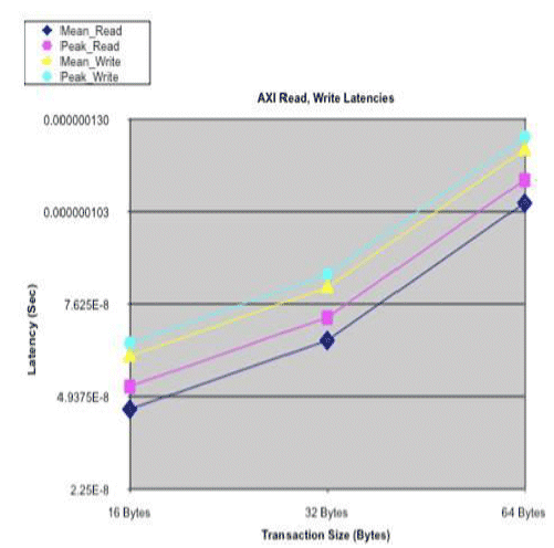
Figure 4b: AXI Read/Write Latencies
The AHB Bus latencies start out lower than the AXI Bus at 16 Byte transaction size and the AHB Bus does not exceed the AXI Bus at 64 Byte transaction size. Based on the plot trends, one can guesstimate that the AXI Bus should have lower latencies above 128Byte transaction sizes, by changing the Transaction_Size_Bytes parameter and rerunning the model. Note: the y-axis scaling differs.
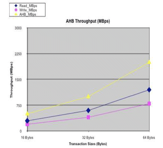
Figure 5a: AHB Throughput
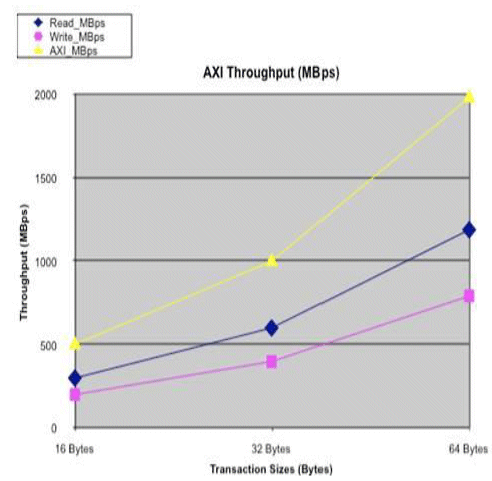
Figure 5b: AXI Throughput
The throughput plots are identical, which is expected if both have the same source traffic rates and sizes. Note: the y-axis scaling differs.
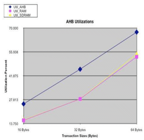
Figure 6a: AHB Utilization
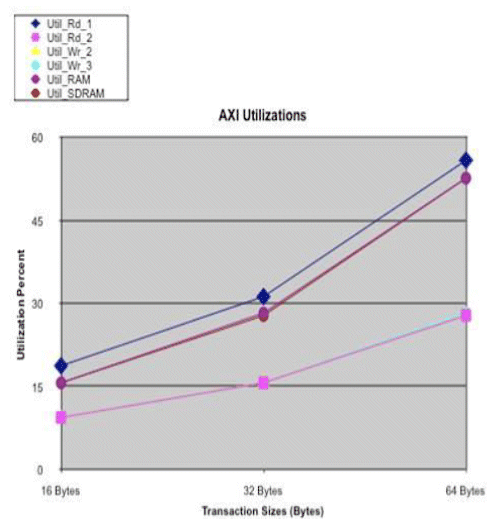
Figure 6b: AXI Utilization
The AHB Bus utilization is higher than the AXI Bus channels for all transaction sizes, which is expected since the AXI Bus has six channels. The percentage values for the AXI Bus do not track the AHB Bus, since it is running at one-half the speed, width of the AHB Bus. Note: the y-axis scaling differs.
Analysis
The system design environment was able to provide the necessary plots to compare the two busses. The latency plots show that the AHB Bus can provide comparable, or lower, latencies up to 64 Byte transaction sizes. The AHB Bus is running at twice the speed, double the width. The throughputs are the same, given the same traffic sources. The utilizations are higher for the AHB Bus, as the AXI Bus has six read/write channels. In terms of power, the single AHB should be approximately 4X a single AXI Bus channel, given the speed and width. Since there are six AXI Bus channels, plus some additional channels, the AXI Bus should consume approximately 1.5X the power of the AHB Bus.
Design Impacts
As a result of this bus model comparison, some bus design considerations emerge:
- Consider the peak utilization of a bus channel. If the model shows the peak loading is in the 70% to 80% range, then the bus can sustain additional traffic without redesign.
- Consider the peak latency for a critical path, such as uProcessor to RAM.
- Will the peak latency allow the design to meet its overall timing objectives, such as a video frame rate?
- Consider the power consumption of the bus topology. Can a shared bus reduce power consumption?
Results
The AHB Bus performed best for the given traffic rates and sizes. The AXI Bus was rated higher for throughput, even though the comparison was the same for both models, since it has additional capacity. The AXI Bus would use approximately 50% more power, assuming similar process technology, again giving the edge to the AHB Bus.
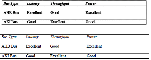
Table 2: Results of the simulation study between AMBA AHB and AMBA AXI
About the author
Deepak Shankar is president of Mirabilis Design, Inc. Shankar has an MBA from UC Berkeley, MS from Clemson University and BS from Coimbatore Institute of Technology, both in Electronics and Communication.
Related Semiconductor IP
- AXI Bridge with DMA for PCIe IP Core
- PCIe 7.0 Controller with AXI
- Multi-Channel AXI DMA Engine
- AXI Bridge for PCIe IP Core
- Siemens EDA* AXI Verification IP Suite
Related White Papers
- 8051s in Modern Systems: Interfacing to AMBA Buses
- Amba bus may move MIPS into ARM territory
- Delivering verified AMBA AXI systems-on-chips
- Designing Using the AMBA (TM) 3 AXI (TM) Protocol -- Easing the Design Challenges and Putting the Verification Task on a Fast Track to Success
Latest White Papers
- Ramping Up Open-Source RISC-V Cores: Assessing the Energy Efficiency of Superscalar, Out-of-Order Execution
- Transition Fixes in 3nm Multi-Voltage SoC Design
- CXL Topology-Aware and Expander-Driven Prefetching: Unlocking SSD Performance
- Breaking the Memory Bandwidth Boundary. GDDR7 IP Design Challenges & Solutions
- Automating NoC Design to Tackle Rising SoC Complexity