IMEC sets major step towards 3D integration of DRAM on logic
Leuven, Belgium – Ocotober 1, 2009 – IMEC and its 3D integration partners have taped-out Etna, a new 3D chip integrating a commercial DRAM chip on top of a logic IC. The new 3D stack resembles as close as possible to future commercial chips. It consists of a 25µm thick logic die on top of which a commercial DRAM is stacked using through-silicon vias (TSVs) and micro-bumps.
The 3D demonstrator mimics all aspects of the approach by stacking an advanced commercial DRAM product chip on IMEC’s proprietary CMOS logic IC. As an example, heaters are integrated to test the impact of hotspot on DRAM refresh times. And, the chip contains test structures for monitoring thermo-mechanical stress in a 3D stack, ESD (electro-static discharge) hazards, electrical characteristics of TSVs and micro-bumps, fault models for TSVs, etc.
The design of the 3D chip is realized together with many players in the 3D integration supply chain. Now, IMEC is manufacturing the logic die in its prototype line, and will be stacking the commercial DRAM chip on top of it. One of IMEC’s 3D integration partners will deliver the DRAM dies, and will test the fabricated 3D stack; two other partners, will package the 3D stack using flip-chip onto a FBGA (fine-pitch ball-grid array) substrate.
“We are excited to achieve this milestone in collaboration with our 3D integration partners including memory suppliers and IC manufacturers. This test-chip is a significant step for the introduction of 3D technology in DRAM-on-logic applications;” said Pol Marchal, principal scientist 3D integration at IMEC.
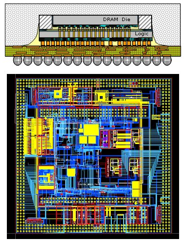
ETNA 3D chip stack paving the way for DRAM on logic integration; (top) stack configuration; (bottom) layout of the logic die
About IMEC
IMEC is a world-leading independent research center in nanoelectronics and nanotechnology. IMEC is headquartered in Leuven, Belgium, and has offices in Belgium, the Netherlands, Taiwan, US, China and Japan. Its staff of more than 1,650 people include over 550 industrial residents and guest researchers. In 2008, IMEC's revenue (P&L) was 270 million euro.
IMEC's More Moore research targets semiconductor scaling for the 22nm technology node and beyond. With its More than Moore research, IMEC invents technology for nomadic embedded systems, wireless autonomous transducer solutions, biomedical electronics, photovoltaics, organic electronics and GaN power electronics.
IMEC's research bridges the gap between the fundamental research at universities and R&D in the industry. It has unique processing and system know-how, intellectual property portfolio, state-of-the-art infrastructure, and a strong and worldwide network position. This makes IMEC a key partner for shaping the technology of the future.
Further information on IMEC can be found at www.imec.be.
Related Semiconductor IP
- UCIe D2D Adapter & PHY Integrated IP
- Low Dropout (LDO) Regulator
- 16-Bit xSPI PSRAM PHY
- ASIL B Compliant MIPI CSI-2 CSE2 Security Module
- SHA-256 Secure Hash Algorithm IP Core
Related News
- Synopsys 3DIC Compiler Qualified for Samsung Foundry's Multi-Die Integration Flow, Accelerating 2.5D and 3D Designs
- Nano Labs Launches FPU3.0 ASIC Design Architecture with 3D DRAM Stacking for AI and Blockchain Innovation
- InPsytech Tapes Out F2F SoIC Design Compliant with UCIE 2.0 Standard Enabling High-Speed Interconnects for 3D Heterogeneous Integration
- d-Matrix and Alchip Announces Collaboration on World's First 3D DRAM Solution to Supercharge AI Inference
Latest News
- EU DARE Project Is Scrambling to Replace Codasip
- Sofics and Alcyon Photonics Partner to Support Next-Generation Photonic Systems
- QuickLogic Appoints Quantum Leap Solutions as Authorized Sales Representative
- Cadence and NVIDIA Expand Partnership to Reinvent Engineering for the Age of AI and Accelerated Computing
- Cadence and Google Collaborate to Scale AI-Driven Chip Design with ChipStack AI Super Agent on Google Cloud