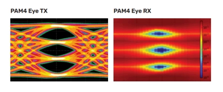
TSMC 16nmFF+ 28G SerDes IP
Filter
Compare
3,575
IP
from
90
vendors
(1
-
10)
-
SerDes IP
- 10dB to 35dB bump-to-bump insertion loss
- Multi-rate support for 56Gbps to 112Gbps PAM4 and NRZ
- Integrated PLL
- Robust clock distribution architecture
- Advanced mixed signal analog equalization architecture
- Fully adaptive and programmable RX equalization
- Auto-negotiation
- Link Training
-
ESD Solutions for Multi-Gigabit SerDes in TSMC 28nm
- A Wirebond and FlipChip compatible <80fF ESD Solutions for Multi-Gigabit SerDes Applications.
- This silicon-proven TSMC 28nm Digital I/O Library delivers a low-capacitance, high-reliability interface solution optimized for advanced semiconductor applications.
- Featuring low-capacitance LVDS differential pairs (<250fF per pin) at 0.8V, this library ensures superior signal integrity for high-speed applications.
-
Programmable Low Power SERDES on TSMC CLN40G
- Programmable SERDES analog front end that supports 1 to 11+ Gbps standard serial protocols
- Compact form factor – 0.104 mm2 active silicon area per lane including ESD
- Industry leading low power – typically 5.8 mW/Gbps including termination
- Minimal latency – 3 UI between parallel transfer and serial transmission
-
Programmable Low Power SERDES on TSMC CLN28HPL
- Programmable SERDES analog front end that supports 1 to 6+ Gbps standard serial protocols
- Compact form factor – 0.095 mm2 active silicon area per lane including ESD
- Industry leading low power – typically 5.6 mW/Gbps including termination
- Minimal latency – 3 UI between parallel transfer and serial transmission
-
PCIe Express Gen4 / Ethernet SERDES on TSMC CLN5A
- Industry leading low power PMA macro – 122.9mW per lane at 16Gbps (7.7mW/Gbps) inclusive of Tx and Rx PLLs, termination, bias, etc.
- Support for Ethernet protocols and Automotive Grade 2
- Compact form factor – 0.34 mm2 active silicon area per lane including ESD
- Minimal latency – 3 UI between parallel transfer and serial transmission
-
PCI Express Gen4 / Ethernet SERDES on TSMC CLN5
- Industry leading low power PMA macro – 122.9mW per lane at 16Gbps (7.7mW/Gbps) inclusive of Tx and Rx PLLs, termination, bias, etc.
- Support for Ethernet protocols and Automotive Grade 2
- Compact form factor – 0.34 mm2 active silicon area per lane including ESD
- Minimal latency – 3 UI between parallel transfer and serial transmission
-
112G-ELR PAM4 SerDes PHY - TSMC 5nm
- TSMC 5nm FinFET CMOS Process
- Power-optimized for ELR and LR links
- Integrated BIST capable of producing and checking PRBS
- 56-112Gbps PAM4 or 1-56Gbps NRZ data rates
-
Multi Rail LDO for SERDES on TSMC CLN3P-CLN3X
- Easy to integrate with no special power requirements
- Easy to use and configure
- Programmable output level
- Trimming supported using 4-bit control
-
Multi Rail LDO for SERDES on TSMC CLN3E
- Easy to integrate with no special power requirements
- Easy to use and configure
- Programmable output level
- Trimming supported using 4-bit control
-
Multi Rail LDO for SERDES on TSMC CLN2P
- Easy to integrate with no special power requirements
- Easy to use and configure
- Programmable output level
- Trimming supported using 4-bit control