Altera Nios II processor IP
Filter
Compare
17
IP
from
3
vendors
(1
-
10)
-
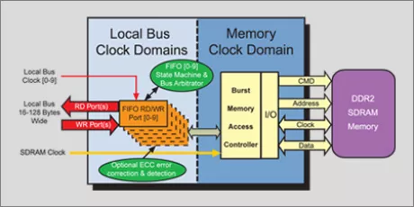
Avalon Multi-port DDR2 Memory Controller
- 200 / 333 MHz (400/666 Mbps) Cyclone/Stratix DDR2 memory performance
- DDR2 Memory Devices
- From 1 to 16 Avalon-MM local bus port interfaces
- Memory bandwidth utilization in excess of 95%
-
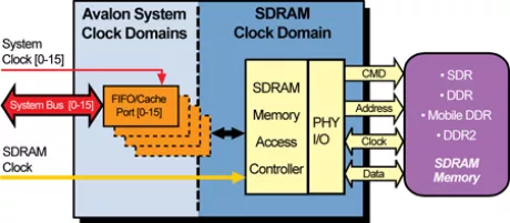
Avalon Multi-port SDRAM Memory Controller IP Core
- 200 / 333 MHz (400/666 Mbps) Cyclone / Stratix DDR2 memory performance
- SDR, DDR, DDR2 and Mobile DDR SDRAM Memory Devices
- From 1 to 16 Avalon-MM local bus port interfaces
- Memory bandwidth utilization in excess of 95%
-
I2C Controller IP – Master, Parameterized FIFO, Avalon Bus
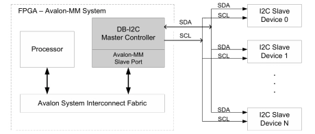
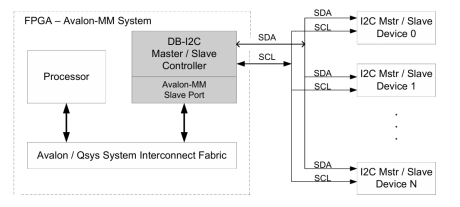
- The DB-I2C-M-AVLN Controller IP Core interfaces a microprocessor via the Avalon Bus to an I2C Bus. The I2C is a two-wire bidirectional interface standard (SCL is Clock, SDA is Data) for transfer of bytes of information between two or more compliant I2C devices, typically with a microprocessor behind the master controller and one or more slave devices.
- The DB-I2C-M-AVLN is a Master I2C Controller that controls the Transmit or Receive of data to or from slave I2C devices. In an Altera FPGA, typically, the microprocessor is a NIOS II processor, but can be any FPGA embedded processor. Figure 1 depicts the system view of the DB-I2C-M-AVLN Controller IP Core embedded within an FPGA integrated circuit device.
-
I2C Controller IP- Master / Slave, Parameterized FIFO, Avalon Bus
- The DB-I2C-MS-AVLN Controller IP Core interfaces a microprocessor via the Avalon Bus to an I2C Bus in Standard-Mode (100 Kbit/s) / Fast-Mode (400 Kbit/s) / Fast-Mode Plus (1 Mbit/s) / Hs-Mode (3.4+ Mb/s) / Ultra Fast-Mode (5 mbit/s).
- The I2C is a two-wire bidirectional interface standard (SCL is Clock, SDA is Data) for transfer of bytes of information between two or more compliant I2C devices, typically with a microprocessor behind the master controller and one or more slave devices.
- The DB-I2C-MS-AVLN is a Master / Slave I2C Controller that in Master Mode controls the Transmit or Receive of data to or from slave I2C devices while in Slave Mode allows an external I2C Master device to control the Transmit or Receive of data.
-
I2C Master
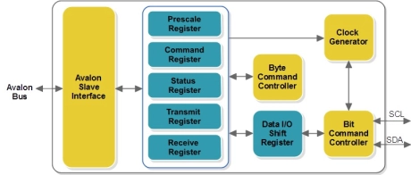
- Avalon compliant I²C Master IP core provides an interface between Nios II processor and an I²C Slave device.
- It can work as a master transmitter or master receiver depending on working mode determined by Nios II processor.
- The I²C Master IP core incorporates all features required by the latest I²C specification including clock synchronization, arbitration, multi-master systems and fast-speed transmission mode.
-
I2C Controller
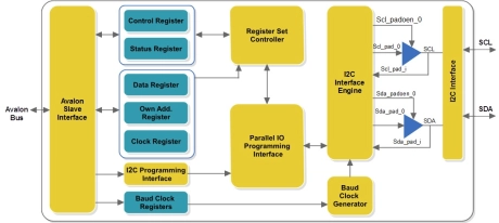
- I²C (Inter-Integrated Circuit) Controller is a two-wire, bi-directional serial bus that provides simple and efficient method of data transmission over a short distance between many devices.
- Avalon compliant I²C Controller provides an interface between Nios II processor and I²C device.
- It can work as Master/Slave transmitter or Master/Slave receiver depending on working mode determined by Nios II processor.
-
SPI Controller IP- Master/ Slave, Parameterized FIFO, Avalon Bus
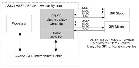
- The Digital Blocks DB-SPI-MS-AVLN is a Serial Peripheral Interface (SPI) Controller Verilog IP Core supporting both Master/Slave SPI Bus transfers.
- The DB-SPI-MS contains an Avalon Bus Interface for interfacing a microprocessor to external SPI Master/Slave devices.
-
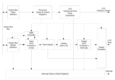
Display Controller – LCD / OLED Panels (Avalon Bus)
- The DB9000AVLN TFT LCD Controller IP Core interfaces a microprocessor and frame buffer memory via the Avalon Bus within Altera Qsys Integration (generating the System Interconnect Fabric) to a TFT LCD panel.
- In an Altera FPGA, typically, the microprocessor is a NIOS II or ARM processor and frame buffer memory is either on-chip SRAM memory or larger off-chip SRAM or SDRAM.
-
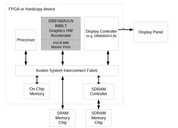
BitBLT Graphics Hardware Accelerator (Avalon Bus)
- The DB9100AVLN BitBLT Graphics Hardware Accelerator Verilog IP Core renders a graphics frame by generating new bitmaps from commands to combining existing bitmaps on and off-screen using one of 256 Raster Operations.
- A Raster Operation (ROP) is a bitwise Boolean operation (such as AND, OR, XOR, NOT).
-
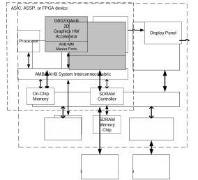
2D Graphics Hardware Accelerator (AHB Bus)
- Generates bitmaps from graphics instructions as well as combining existing bitmaps on and off-screen using one of 256 Raster Operations. A Raster Operation (ROP) is a bitwise Boolean operation (such as AND, OR, XOR, NOT) which lay the foundation for power hardware graphics primitive operations
- Generates characters from compressed bitmaps using its FONT Bitmap Color Expansion Unit
- Performs Alpha Blend operations of bitmaps with its Alpha Blend unit
- Draws lines, polygons, circles using its hardware efficient & pixel accurate Bresenham Algorithm Line Drawing Unit