DDR5 PHY IP
Welcome to the ultimate DDR5 PHY IP hub! Explore our vast directory of DDR5 PHY IP
All offers in
DDR5 PHY IP
Filter
Compare
360
DDR5 PHY IP
from
18
vendors
(1
-
10)
-
High Speed DDR Interface Solution
- Brite provides a complete DDR subsystem including not only controller, PHY and IO, but also corresponding tuning and configuration software. And this solution can support LPDDR2, DDR3, LPDDR3, DDR4 and LPDDR4/4x combo PHY with the data rate from 667Mbps to 4266Mbps.
-
DDR5 MRDIMM PHY and Controller
- The DDR5 12.8Gbps MRDIMM Gen2 PHY and controller memory IP system solutions double the performance of DDR5 DRAM.
- The DDDR5 12.8Gbps design and architecture address the need for greater memory bandwidth to accommodate unprecedented AI processing demands in enterprise and data center applications, including AI in the cloud.
-
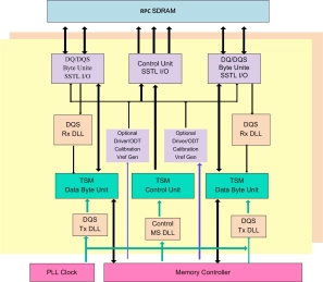
PSRAM/RPC PHY & Controller
- The DDR IP Mixed-Signal MR PSRAM PHY and RPC PHY provide turnkey physical interface solutions for ICs requiring access to JEDEC compatible PSRAM/RPC devices
- It is optimized for low-power and high-speed applications with robust timing and small silicon area
- The PSRAM PHY supports AP memory UHS/OPI PSRAM components on the market, and the RPC PHY supports ETRON components on the market
-
GDDR6X/6 Combo PHY & Controller
- The GDDR6X/6 PHY is fully compliant with the JEDEC GDDR6X/6 standard, supporting data rates of up to 20Gbps per pin for PAM2 GDDR6 mode and 24Gbps for PAM4 GDDR6X mode
- The GDDR6X/6 interface supports 2 channels, each with 16 bits for a total data width of 32 bits per memory device
- With a maximum speed of 20/24Gbps per pin, The GDDR6X/6 Combo PHY delivers a peak bandwidth of up to 80GB/s or 96GB/s per memory device
-
GDDR6 PHY IP for 12nm
- JEDEC JESD250 compliant GDDR6 support
- X16 mode, X8 mode, and pseudo-channel mode
- Low frequency RDQS mode support
-
LPDDR5X/5/4X/4 PHY IP for 12nm
- Compliant with JEDEC standards for LPDDR5X/5/4X/4 with PHY standards
- DFI 5.0 Interface Compliant
- Supports up to 4 ranks
- Multiple frequency states

-
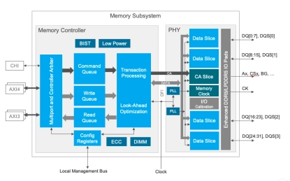
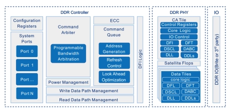
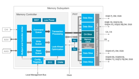
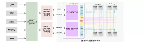
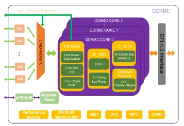
DDR5 IP solution
- Compatible with DDR5 up to 4800Mbps
- AXI compliant multi-ports, and data width, FIFO depth, command queue depth configurable
- DFI5.0/4.0 compliant interface between controller and PHY
- Support ECC (error correcting code)
-
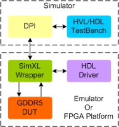
GDDR5 Synthesizable Transactor
- Supports 100% of GDDR5 protocol standard JESD212C
- Supports all the GDDR5 commands as per the specs
- Supports all types of timing and protocol violation detection
- Supports up to 8GB device density
-
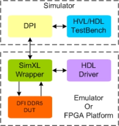
DDR5 DFI Synthesizable Transactor
- Compliant with DFI 5.0 Specification.
- DFI-DDR5 Applies to :
- DDR5 protocol standard JESD79-5 & JESD79-5 Rev1.40 (Draft) Specifications
- Supports all Interface Groups.
-
DDR PHY
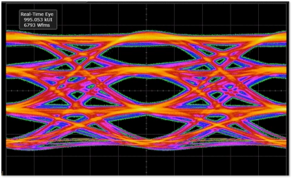
- DDR5/4/3 training with write-leveling and data-eye training
- Optional clock gating available for low-power control
- Internal and external datapath loop-back modes
- I/O pads with impedance calibration logic and data retention capability
- Programmable per-bit (PVT compensated) deskew on read and write datapaths
- RX and TX equalization for heavily loaded systems